3D NAND memory and manufacturing method thereof
A 3D NAND and memory technology, applied in semiconductor devices, electrical solid state devices, electrical components, etc., can solve the problems of poor electrical performance of 3D NAND memory, low storage density of 3D NAND memory, unstable distribution range of read current, etc., and reach the current fluctuation range Effects of small, stable threshold voltage Vth, and stable reading current ID
- Summary
- Abstract
- Description
- Claims
- Application Information
AI Technical Summary
Problems solved by technology
Method used
Image

Examples
Embodiment Construction
[0057] Before introducing the specific embodiments of the present application, the Chinese and English translations and abbreviations of technical terms used in describing the specific embodiments of the present application are firstly introduced.
[0058] Atomic layer deposition: atom layer deposition, ALD;
[0059] Chemical vapor deposition: chemical vapor deposition, CVD;
[0060] Physical vapor deposition: Physical Vapor Deposition, PVD;
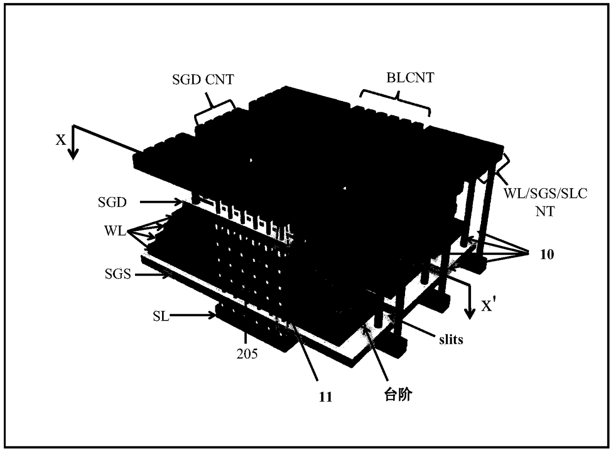
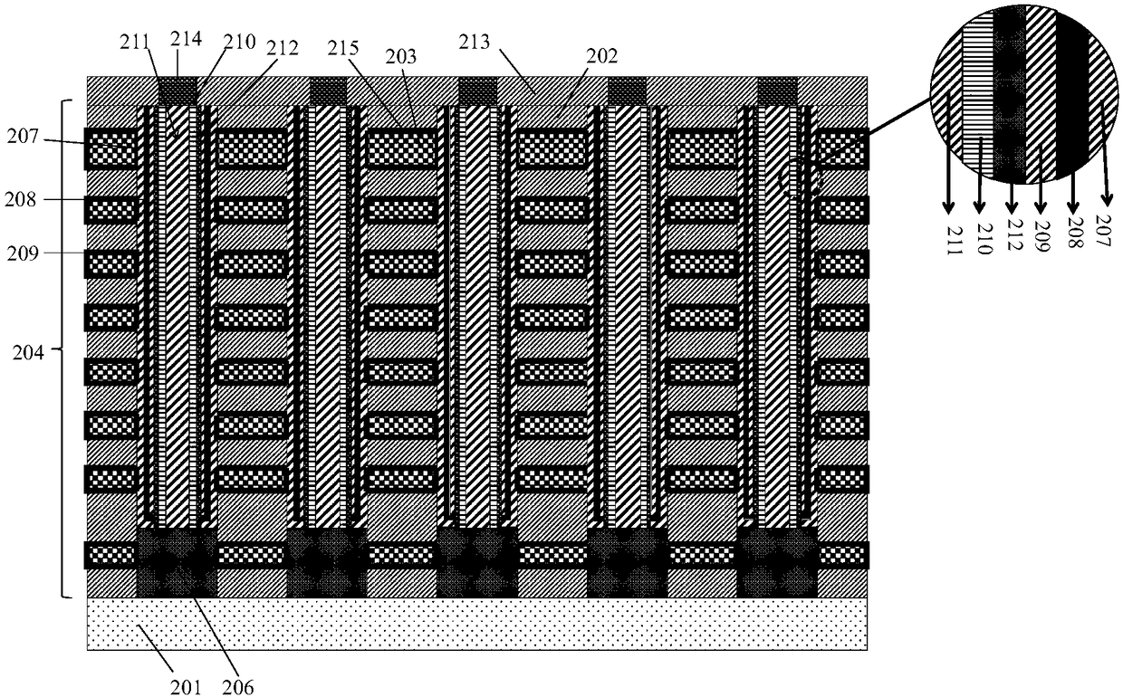
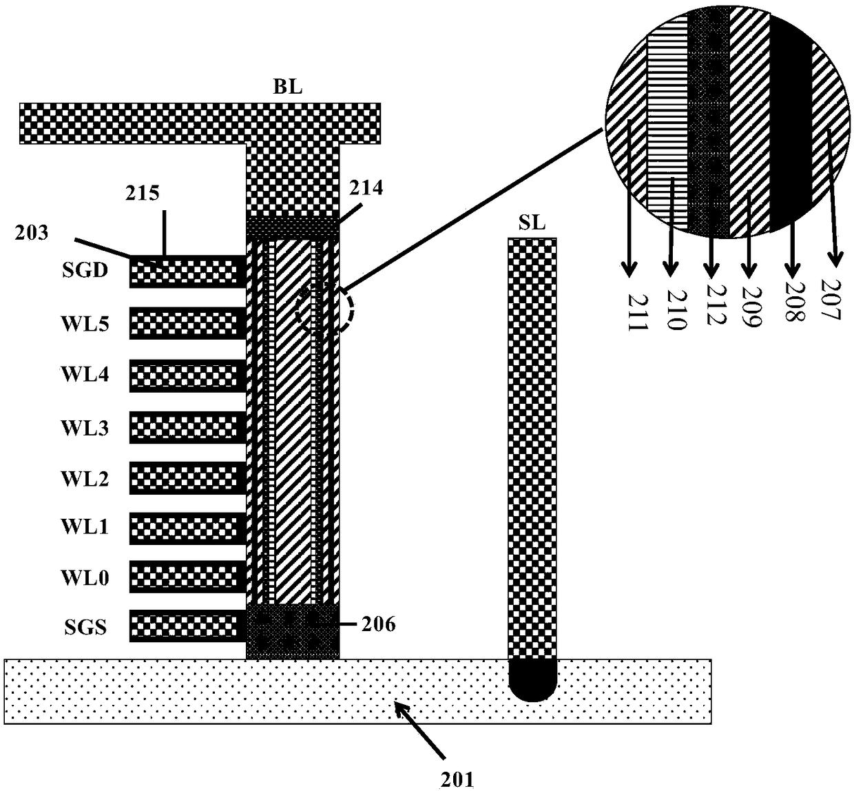
[0061] Source selection gate: Select Gate on Source Side, SGS;
[0062] Drain selection gate: Select Gate on Drain Side, SGD;
[0063] Bit line: bit line, BL;
[0064] Word line: word line, WL;
[0065] Source: source line, SL.
[0066] Based on the background technology, it can be seen that the existing 3D NAND memory has the following problems: poor electrical performance, low read / write efficiency, and low storage density.
[0067]The inventors of the present application have discovered through research that the above-mentioned ...
PUM
 Abstract
Description
Claims
Application Information
 - R&D
- Intellectual Property
- Life Sciences
- Materials
- Tech Scout
- Unparalleled Data Quality
- Higher Quality Content
- 60% Fewer Hallucinations
Browse by: Latest US Patents, China's latest patents, Technical Efficacy Thesaurus, Application Domain, Technology Topic, Popular Technical Reports.
© 2025 PatSnap. All rights reserved.Legal|Privacy policy|Modern Slavery Act Transparency Statement|Sitemap|About US| Contact US: help@patsnap.com