A method for preparing a hemt device nano-gate

A device and nanotechnology, which is applied in the field of preparation of nanometer gates of HEMT devices, can solve the problems of complex process and expensive equipment, and achieve the effects of simple process, low cost and small gate electrode.

Active Publication Date: 2020-12-22
SOUTH CHINA UNIV OF TECH
View PDF6 Cites 0 Cited by
  • Summary
  • Abstract
  • Description
  • Claims
  • Application Information

AI Technical Summary

Problems solved by technology

[0011] In order to overcome the above-mentioned shortcomings and deficiencies of the prior art, the object of the present invention is to provide a method for preparing a nano-gate of a HEMT device, which solves the problem of complex and expensive equipment in the prior art, and realizes the simple and convenient fabrication of high-frequency and high-power HEMT devices. preparation

Method used


Image

  • A method for preparing a hemt device nano-gate
  • A method for preparing a hemt device nano-gate
  • A method for preparing a hemt device nano-gate

Examples


Embodiment 1

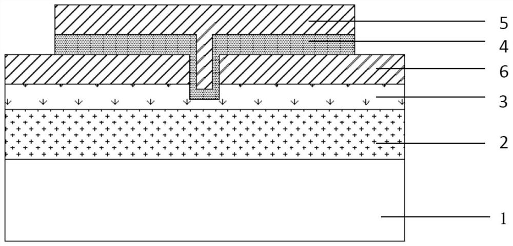
[0045] In the preparation method of the HEMT device nano-gate of the present embodiment, in the manufacturing process of the HEMT device, Ag nanowires are used as a mask to deposit metal on the source and drain electrodes; 3 ·H 2 O, H 2 o 2 、H 2 The method of ultrasonic cleaning of O mixed solution removes the Ag nanowires, forms a slit equivalent to the size of the Ag nanowires between the source and drain electrodes, and finally prepares a nano-gate electrode in the slit, which specifically includes the following steps:

[0046] (1) Clean the surface of the HEMT heterojunction epitaxial wafer: use acetone, ethanol, O 2 The method of plasma purging is cleaned;

[0047] (2) The ethanol solution dispersed with Ag nanowires is slowly dropped on the surface of the HEMT epitaxial wafer, and the ethanol is completely volatilized; the diameter of the Ag nanowires is 80nm, and the length is 100um;

[0048] (3) the epitaxial wafer that step (2) obtains is placed in 10 -5In the v...

Embodiment 2

[0062] In the preparation method of the HEMT device nano-gate of the present embodiment, in the manufacturing process of the HEMT device, Ag nanowires are used as a mask to deposit metal on the source and drain electrodes; 3 ·H 2 O, H 2 o 2 、H 2 The method of ultrasonic cleaning of O mixed solution removes the Ag nanowires, forms a slit equivalent to the size of the Ag nanowires between the source and drain electrodes, and finally prepares a nano-gate electrode in the slit, which specifically includes the following steps:

[0063] (1) Clean the surface of the HEMT heterojunction epitaxial wafer: use acetone, ethanol, O 2 The method of plasma purging is cleaned;

[0064] (2) The ethanol solution dispersed with Ag nanowires is slowly dropped on the surface of the HEMT epitaxial wafer, and the ethanol is completely volatilized; the diameter of the Ag nanowires is 50nm, and the length is 50um;

[0065] (3) the epitaxial wafer that step (2) obtains is placed in 10 -5 In the v...

Embodiment 3

[0074] In the preparation method of the HEMT device nano-gate of the present embodiment, in the manufacturing process of the HEMT device, Ag nanowires are used as a mask to deposit metal on the source and drain electrodes; 3 ·H 2 O, H 2 o 2 、H 2 The method of ultrasonic cleaning of O mixed solution removes the Ag nanowires, forms a slit equivalent to the size of the Ag nanowires between the source and drain electrodes, and finally prepares a nano-gate electrode in the slit, which specifically includes the following steps:

[0075] (1) Clean the surface of the HEMT heterojunction epitaxial wafer: use acetone, ethanol, O 2 The method of plasma purging is cleaned;

[0076] (2) Slowly drop the ethanol solution dispersed with Ag nanowires on the surface of the HEMT epitaxial wafer, until the ethanol is completely volatilized; the Ag nanowires have a diameter of 100nm and a length of 200um;

[0077] (3) the epitaxial wafer that step (2) obtains is placed in 10 -5 ~10 -6 In th...


PUM

PropertyMeasurementUnit
diameteraaaaaaaaaa
lengthaaaaaaaaaa
thicknessaaaaaaaaaa

Abstract

The invention discloses a HEMT device nanometer grid electrode preparation method; in the HEMT device making process, an Ag nano wire is employed as a mask to make source drain electrode metal depositions; the method also comprises the steps of: using an NH3.H2O, H2O2, and H2O mixture solution ultrasonic cleaning method to remove Ag nano wire; forming a slit between the source electrode and drainelectrode, wherein the slit and the Ag nano wire are equivalent in dimensions; finally, making a nanometer grid electrode in the slit. The formed HEMT device has a low grid source conduction resistance, a high power density and frequency response, is simple in process, low in cost, and can provide important meanings for realizing a high performance nitride-based device.

Description

technical field [0001] The invention relates to a method for preparing a high electron mobility transistor (HEMT), in particular to a method for preparing a nano-gate of a HEMT device. Background technique [0002] Based on Al X Ga 1-X High electron mobility transistors with N / GaN heteroepitaxial structure have broad application prospects in many fields such as high-power microwave communication, radar detection, high-speed transportation, and fast power conversion. The new generation of microwave power electronic devices requires higher response frequency, power density and work efficiency. Due to the HEMT device cut-off frequency f T =v s / (2πL), the most direct way to increase the device cut-off frequency is to reduce the gate length L. Therefore, to further improve the performance of HEMT devices, the main method currently used is to reduce the size of the device, reduce the source-drain distance and the gate length, thereby reducing the migration distance of electr...

Claims


Application Information

Patent Timeline
Patent Type & Authority Patents(China)
IPC IPC(8): H01L29/778H01L21/336
CPCH01L29/66431H01L29/66462H01L29/778
Inventor 李国强陈丁波刘智崑万利军
Owner SOUTH CHINA UNIV OF TECH
Why Eureka
Try Eureka