Electrically programmable fuse structure and semiconductor device
A fuse structure and device technology, applied in semiconductor devices, electric solid state devices, semiconductor/solid state device components, etc., can solve the problems of device influence and fuse chain burst, reduce the heat dissipation process, reduce the risk of burst, The effect of speeding up the rate of fusing
- Summary
- Abstract
- Description
- Claims
- Application Information
AI Technical Summary
Problems solved by technology
Method used
Image
Examples
Embodiment 1
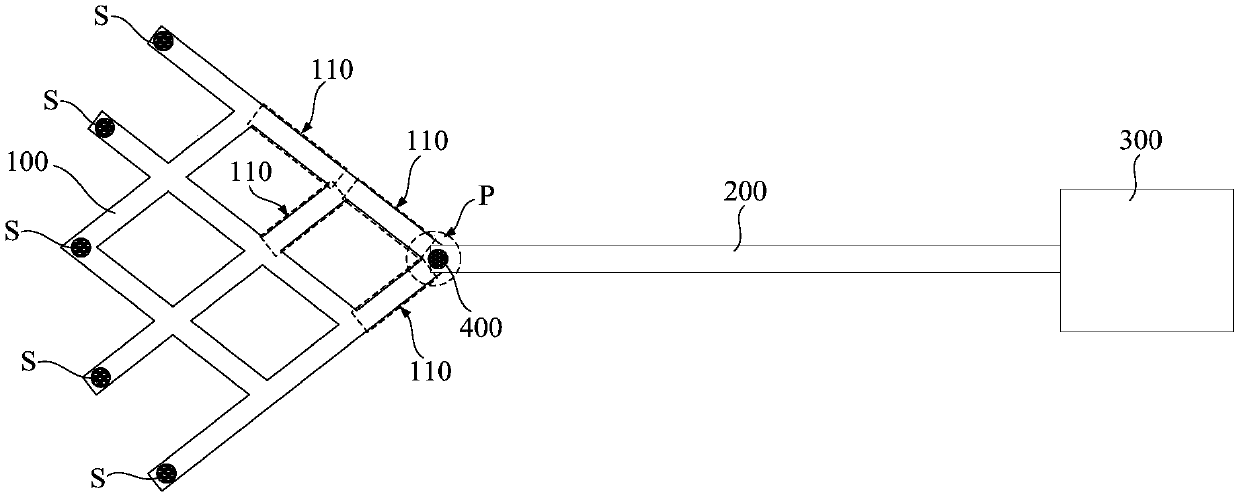
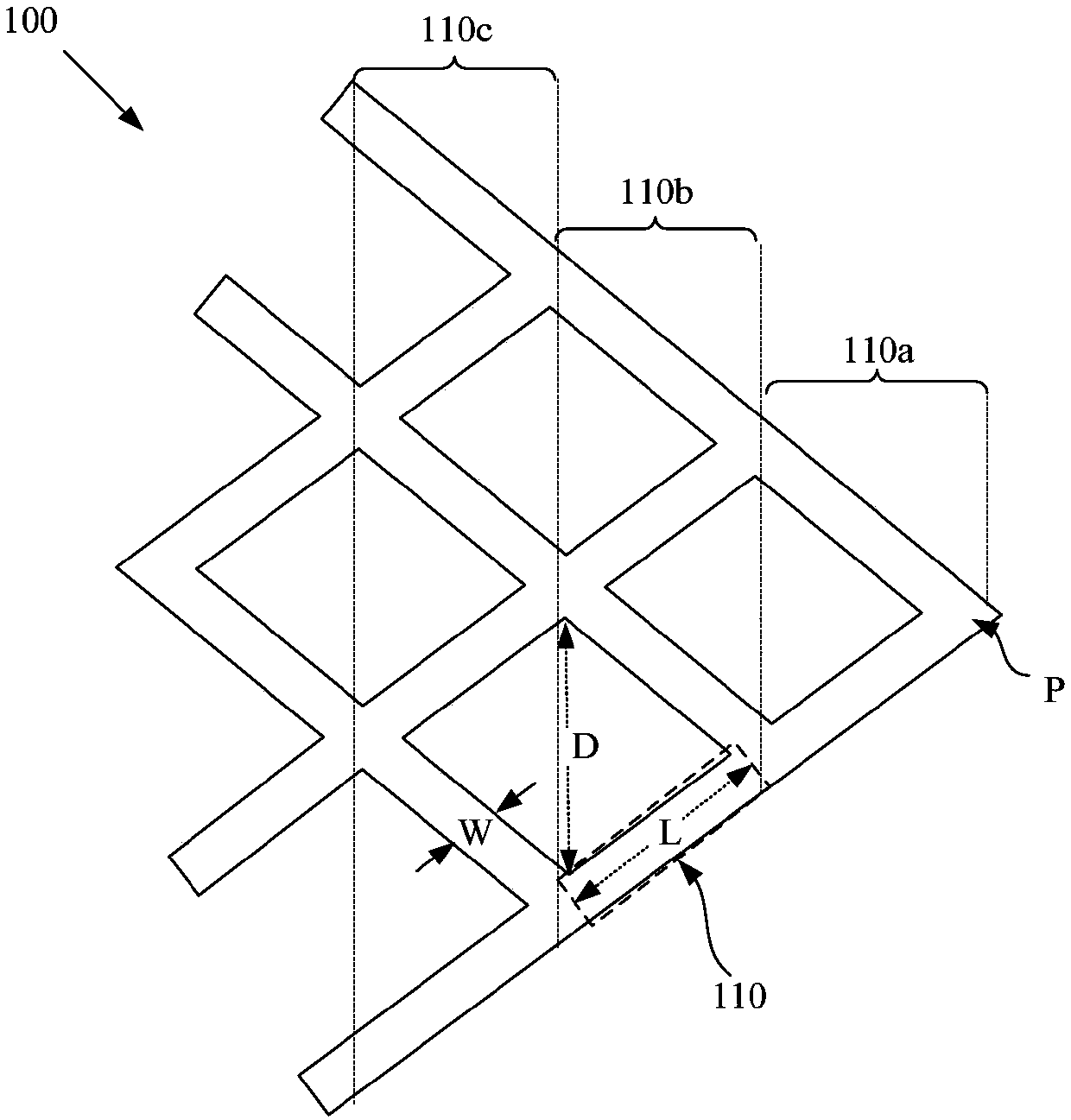
[0057] Figure 2a is a schematic diagram of the electric programmable fuse structure in Embodiment 1 of the present invention, Figure 2b for Figure 2a Shown is a partial enlarged view of the electric programmable fuse structure in Embodiment 1 of the present invention. Such as Figure 2a with Figure 2b As shown, the e-fuse structure includes a cathode 100 and a fuse link 200 , one end of the cathode 100 and the fuse link 200 are connected to each other and have a connection point P. And, the electric programmable fuse structure further includes an anode 300 , and the anode 300 is connected to the other end of the fuse link 200 . Wherein, the material of the cathode 100 includes metal, for example. The fuse link 200 can be a single-layer structure or a laminated structure; and, the material of the fuse link 200 can also include metal, that is, the fuse link 200 can be a single-layer metal layer, or it can be for laminated metal layers. The forming process of the fuse ...
Embodiment 2
[0083] The difference from Embodiment 1 is that the shape of the cathode in this embodiment presents a comb-like structure or a tree-like structure. And, the cathode can also be a symmetrical structure with the length direction of the fuse link as the axis direction.
[0084] Figure 3a It is a schematic diagram of the electric programmable fuse structure in Embodiment 2 of the present invention, Figure 3b for Figure 3a The partial enlarged view of the electric programmable fuse structure in the second embodiment of the present invention is shown. to combine Figure 3a with Figure 3b As shown, in this embodiment, the plurality of conductive branches 110' of the cathode 100' can also be divided into N branch groups, and the conductive branches 110' in the first branch group 110a' are connected to the connection point P, and the first The conductive branches 110' in the N branch groups are connected to the conductive branches 110' in the N-1th branch group. And, the num...
Embodiment 3
[0090] Based on the above-mentioned electrically programmable fuse structure, the present invention also provides a semiconductor device, which includes the electrically programmable fuse structure. For example, the semiconductor device is a memory, and the memory may further be a dynamic random access memory.
[0091] Wherein, the memory further includes a storage unit. Optionally, the electrically programmable fuse structure may be used to constitute a part of the storage unit of the memory, so as to realize data storage. Specifically, before programming the electrically programmable fuse structure, the initial resistance of the fuse structure is very small. And, when programming the electrically programmable fuse structure, a large current flows through the fuse link to blow the fuse link, thereby multiplying the resistance value of the electrically programmable fuse structure, and the blown fuse link will be permanently remains open, while the unblown fuse link remains o...
PUM
 Abstract
Description
Claims
Application Information
 - R&D
- Intellectual Property
- Life Sciences
- Materials
- Tech Scout
- Unparalleled Data Quality
- Higher Quality Content
- 60% Fewer Hallucinations
Browse by: Latest US Patents, China's latest patents, Technical Efficacy Thesaurus, Application Domain, Technology Topic, Popular Technical Reports.
© 2025 PatSnap. All rights reserved.Legal|Privacy policy|Modern Slavery Act Transparency Statement|Sitemap|About US| Contact US: help@patsnap.com


