Display substrate, display device and production method of display substrate

A technology for display substrates and substrates, applied in electrical components, electrical solid devices, circuits, etc., can solve the problems of high epitaxial layer requirements, loss of precision, unfavorable high-resolution panels, etc. The effect of small position and alignment difficulty

Active Publication Date: 2018-09-04
BOE TECH GRP CO LTD
View PDF4 Cites 18 Cited by
  • Summary
  • Abstract
  • Description
  • Claims
  • Application Information

AI Technical Summary

Problems solved by technology

[0005] The problem existing in the existing technology is: since the Micro-LED device requires an epitaxial layer during production, the requirements for the epitaxial layer are relatively high, and it can only be produced on silicon wafers or sapphire.
The existing technology cannot realize the direct fabrication of LED on the thin film transistor control circuit
Most of the current Micro-LED devices are made of LED and TFT control circuits separately and then aligned and bonded. Since the alignment and bonding will lose a certain amount of precision, it is not conducive to the production of high-resolution panels.

Method used


Image

  • Display substrate, display device and production method of display substrate
  • Display substrate, display device and production method of display substrate
  • Display substrate, display device and production method of display substrate

Examples


Embodiment Construction

[0081] In order to improve the product yield of the display substrate and the resolution of the display device, embodiments of the present invention provide a display substrate, a display device, and a method for manufacturing the display substrate. In order to make the purpose, technical solution and advantages of the present invention clearer, the following examples are given to further describe the present invention in detail.

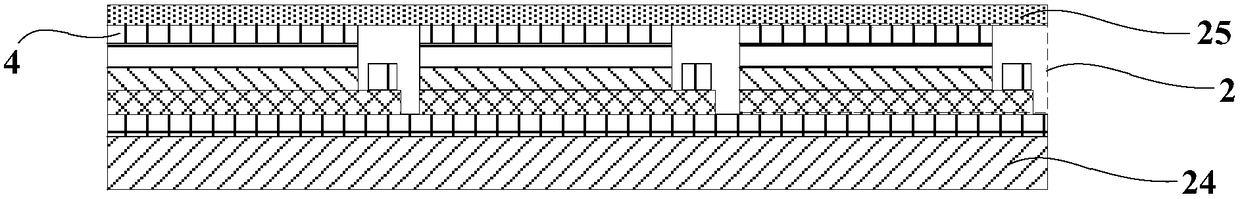
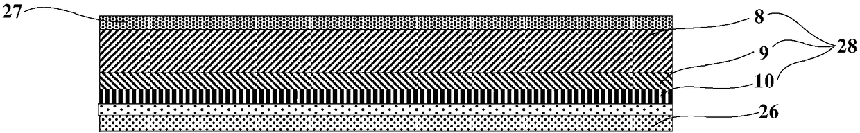
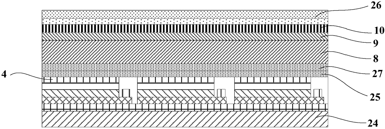
[0082] Such as Figure 7 and Figure 12 As shown, the display substrate provided by the embodiment of the present invention includes: a substrate 1 and a plurality of pixel units arranged in an array arranged on the substrate 1, wherein:

[0083] The pixel unit includes a light emitting diode 2, a connection metal 3 and a thin film transistor 5 arranged in sequence along the direction away from the substrate 1;

[0084] The connecting metal 3 is conductively connected with the top electrode 4 of the light emitting diode 2;

[0085] The active lay...


PUM


Abstract

The invention discloses a display substrate, a display device and a production method of the display substrate. According to the display substrate, the display device and the production method, the product yield of the display substrate and the resolution ratio of the display device are increased. The display substrate comprises a substrate and a plurality of pixel units arrayed on the substrate,wherein the pixel units include a light-emitting diode, a connecting metal and a thin film transistor which are sequentially arranged along the direction far from the substrate; the connecting metal is electrically connected with a top electrode of the light-emitting diode; and an active layer of the thin film transistor is isolated from the connecting metal, and a drain electrode of the thin filmtransistor is conductively connected with the connecting metal.

Description

technical field [0001] The present invention relates to the field of display technology, in particular to a display substrate, a display device and a method for manufacturing the display substrate. Background technique [0002] Micro-LED (Micro Light-Emitting Diode, miniature light-emitting diode) technology, that is, light-emitting diode miniaturization and matrix technology. It refers to a high-density micro-sized LED array integrated on a chip. For example, each pixel of the LED display can be addressed and individually driven to light up. It can be regarded as a miniature version of the outdoor LED display. down to the micron level. [0003] The advantages of Micro-LED are obvious. It inherits the characteristics of high efficiency, high brightness, high reliability and fast response time of inorganic LED, and has the characteristics of self-illumination without backlight. It is more energy-saving, simple in structure and small in size. , thin and other advantages. In...

Claims


Application Information

Patent Timeline
Patent Type & Authority Applications(China)
IPC IPC(8): H01L27/15H01L33/62
CPCH01L27/156H01L33/62H01L33/0093H01L2933/0066H01L25/167H01L33/507H01L33/0054H01L33/34H01L33/502H01L2933/0016H01L2933/0041
Inventor 康昭
Owner BOE TECH GRP CO LTD
Why Eureka
Try Eureka