Photoelectric sensor package and package method thereof

A photoelectric sensor and sealing cover technology, applied in the field of sensors, can solve the problems of insignificant improvement of the thermal noise of the photoelectric sensor and large external size, and achieve the effects of good cooling effect, small external size and small volume

Pending Publication Date: 2018-09-04
PUSU OPTOELECTRONICS TECH SUZHOU CO LTD
View PDF0 Cites 8 Cited by
  • Summary
  • Abstract
  • Description
  • Claims
  • Application Information

AI Technical Summary

Problems solved by technology

[0007] The purpose of the present invention is to provide a photoelectric sensor package to alleviate the technical problems in the prior art that th

Method used


Image

  • Photoelectric sensor package and package method thereof
  • Photoelectric sensor package and package method thereof
  • Photoelectric sensor package and package method thereof

Examples


Embodiment

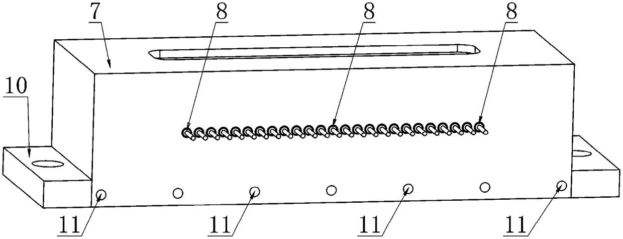
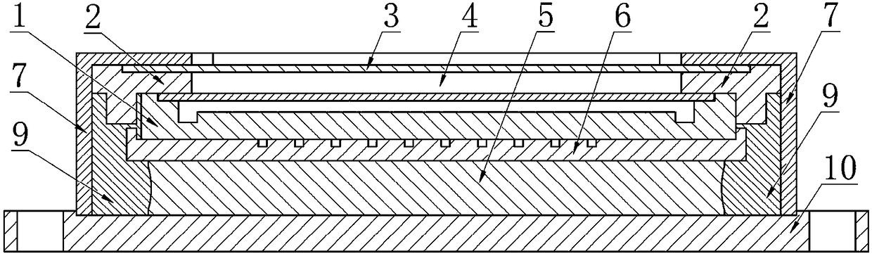
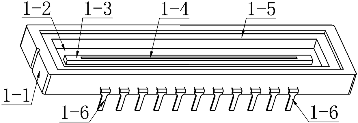
[0048] The structure of the photoelectric sensor in the present embodiment is as follows: as image 3 , the photoelectric sensor in this embodiment takes an array type optical semiconductor detector as an example, which may be a linear array optical semiconductor detector or an area array optical semiconductor detector. The array photoelectric sensor includes a base 1-1, a hollow cavity 1-2 located in the middle of the base, an attachment base 1-3 located at the bottom of the cavity, an array of photosensitive sensing units 1-4 located on the surface of the base, and a sensing unit located on the top of the base. The window transparent sealing sheet 1-5 above the cell array, and the chip pins 1-6 located on both sides of the base.

[0049] In some array photo-semiconductor detectors, the chip pins 1-6 can also be located around the base, or at the edge of the bottom. When the chip pins 1-6 are led out from the edge of the base, they will generally be bent at 90 degrees. But ...


PUM


Abstract

The present invention provides a photoelectric sensor package and a package method thereof, and relates to the field of sensors. The photoelectric sensor package comprises an upper housing with a light transmitting window and a lower housing being in seal connection with the upper housing; the light transmitting window is provided with a light transmitting quartz glass sheet; a location thermal insulation seal cover is arranged between the quartz glass sheet and a photoelectric sensor and is configured to fix the photoelectric sensor and the light transmitting quartz glass sheet, and the location thermal insulation seal cover is internally provided with a cavity configured to hold anhydrous nitrogen and oxygen mixed protection gas; the photoelectric sensor package further comprises a semiconductor refrigeration sheet, a cold end plane of the semiconductor refrigeration sheet is provided with an electromagnetic shielding temperature guidance plate made of metal materials with a good temperature guidance effect, and one side of the electromagnetic shielding temperature guidance plate is butted against the photoelectric sensor to transmit a low temperature at the cold end of the semiconductor refrigeration sheet to the photoelectric sensor.

Description

technical field [0001] The invention relates to the technical field of sensors, in particular to a photoelectric sensor package. The invention also relates to a photoelectric sensor packaging method. Background technique [0002] The photoelectric sensor is a kind of cooling sensor, that is, it needs to work under low temperature conditions. Photoelectric sensors are accompanied by electronic thermal noise during the process of converting optical signals into electrical signals, and this electronic thermal noise is called dark current. Since the existence of dark current affects the detection limit of photoelectric sensors, one of the key factors to ensure the effect of the sensor is to reduce the dark current as much as possible. [0003] Since the higher the operating temperature of the sensor, the greater the dark current, the most effective way to reduce the dark current is to cool down the sensor, so as to reduce the thermal noise of the photoelectric sensor, reduce t...

Claims


Application Information

Patent Timeline
IPC IPC(8): H01L31/0203H01L23/38H01L23/367H01L23/373
CPCH01L23/367H01L23/3738H01L23/38H01L31/0203
Inventor 冯旭东赵振英
Owner PUSU OPTOELECTRONICS TECH SUZHOU CO LTD
Why Eureka
Try Eureka