
Optoelectronic MCM package

a technology of optoelectronic modules and modules, applied in the field of single chip (scm) and multi-chip (mcm) modules, can solve the problems of limited density of interconnects at the electrical side, limited scaling of electrical interconnects, and large size of currently available modules, so as to improve the signal bandwidth density, improve stability, and facilitate lest

Inactive Publication Date: 2008-12-30
IBM CORP
View PDF8 Cites 33 Cited by
  • Summary
  • Abstract
  • Description
  • Claims
  • Application Information

AI Technical Summary

Benefits of technology

[0008]It is an aspect of an embodiment of the present invention to provide a method to integrate optoelectronics onto a single chip module (SCM) or a multi-chip module (MCM) in order to increase the signal bandwidth density to and from the chip as well as the interconnect distance.
[0009]It is another aspect of an embodiment of the present invention to provide an optoelectronic module that is easier to lest than prior art devices.
[0010]It is yet another aspect of an embodiment of the present invention to provide a module package where the electrical and optical components are decoupled which will give the optics better stability.
[0011]It is yet a further aspect of an embodiment of the present invention to provide a short electrical via connection between the processors and the optoelectronic module to mitigate electrical signal interference.

Problems solved by technology

Electrical interconnects exhibit limitations in scaling to even higher bandwidth density in tern-s of the maximum data rate per line, the interconnect distance, power and crosstalk.
However, the currently available modules are large in their size and the interconnect density at the electrical side is limited to the density that is available in standard printed circuit board technology.

Method used


Image

  • Optoelectronic MCM package
  • Optoelectronic MCM package
  • Optoelectronic MCM package

Examples


Embodiment Construction

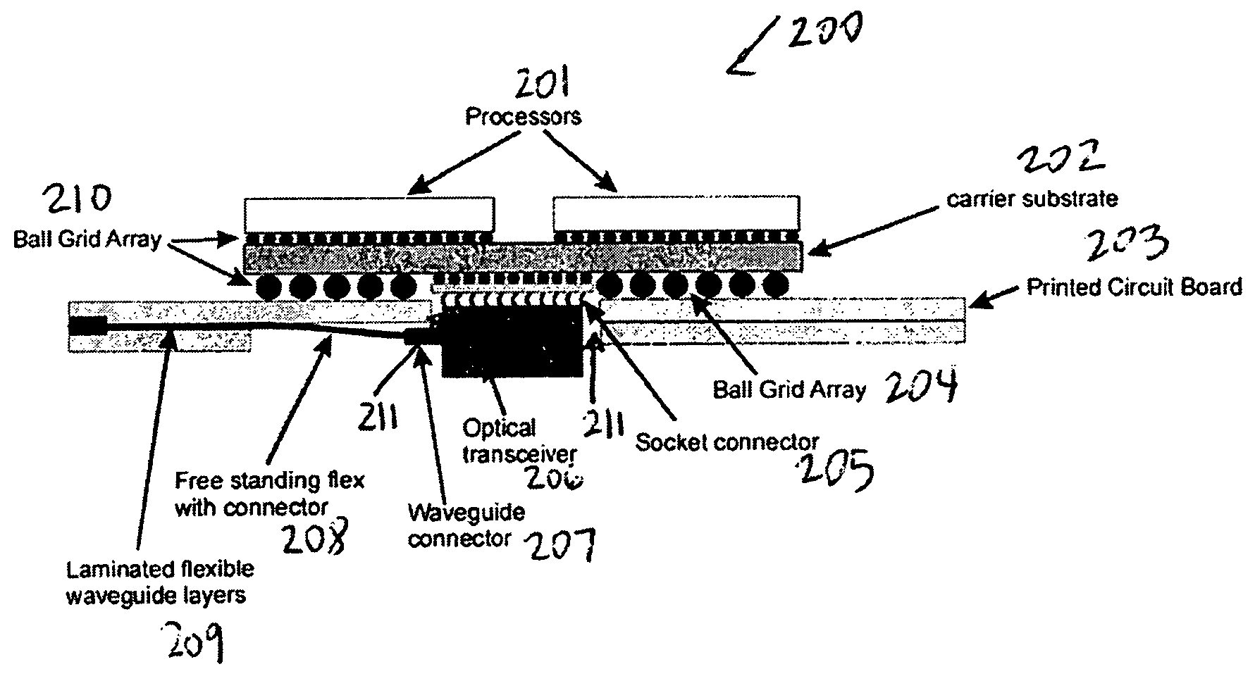
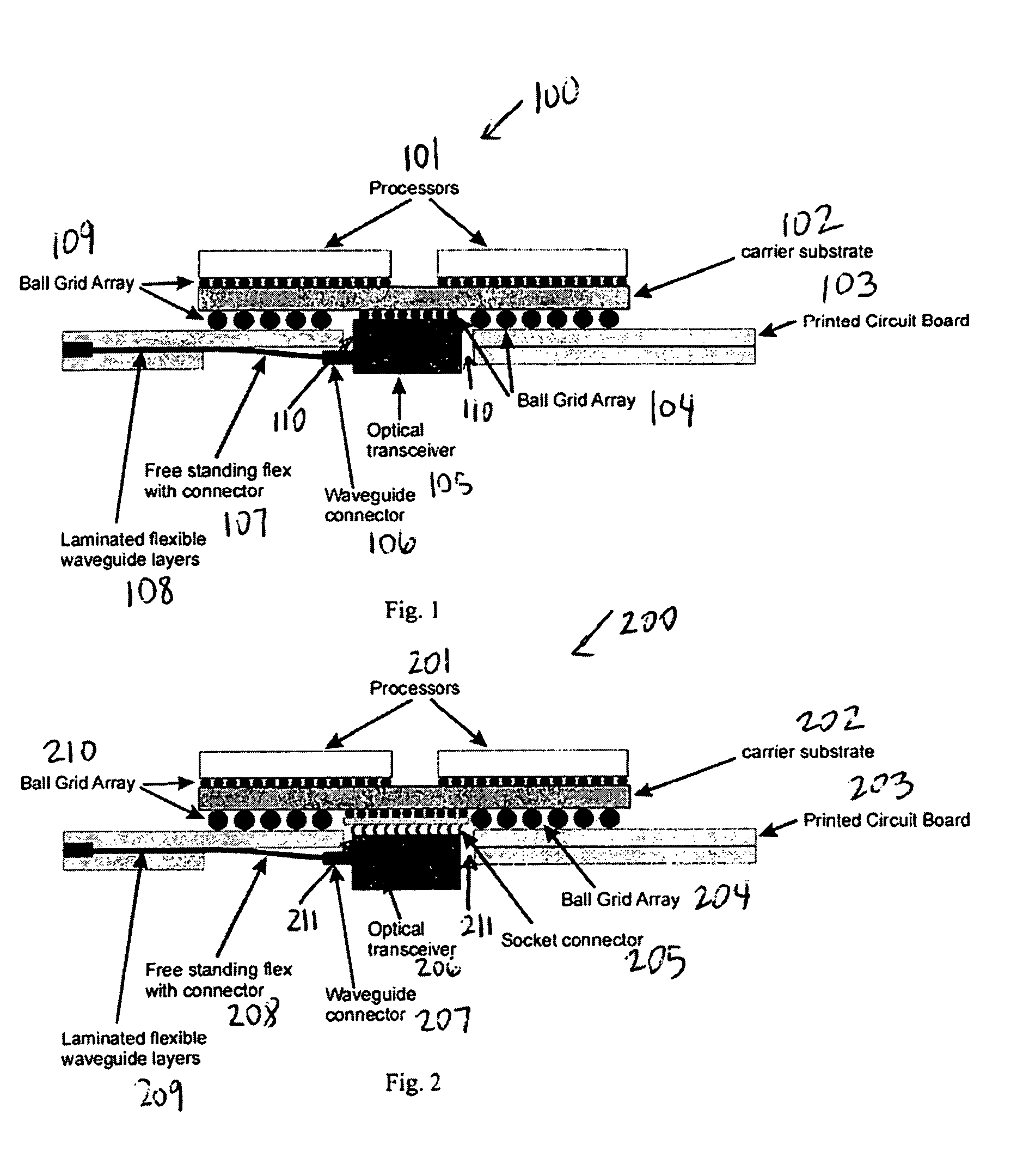
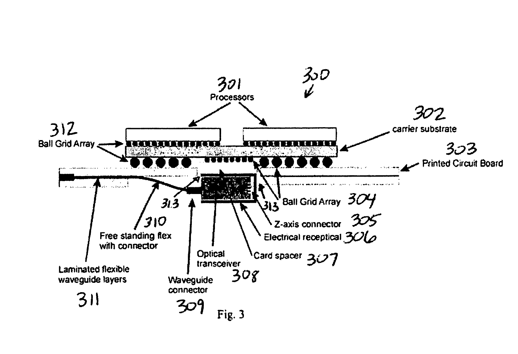
[0016]The present invention will now be described in terms of the embodiment illustrated in FIG. 1. FIG. 1 shows an opto-electronic module or package 100 having processors 101. The processors 101 can be any of those known in the art. Preferably, the processors 101 are high-end processing chips or switch and router chips. Connected to the processors 101 is ball grid array 109. Ball grid array 109 connects the processors 101 to carrier substrate 102. The carrier substrate is connected to the printed circuit board 103 by ball grid arrays 109 and 104. Those skilled in the art will recognize that the present invention may use connectors other than ball grid arrays without departing from the scope of the present invention. Having the processors 101 above the printed circuit board 103 allows for the electronics heat to be dissipated upwards while the heat generated by optical transceiver 105 is dissipated downwards. Optical transceiver 105 is installed in circuit board openings 110. This a...


PUM


Abstract

A structure for electronics package for module packaging and a method of manufacturing a single chip module (SCM) or multi-chip module (MCM) for an opto-electronic package having an improved structure for heat dissipation and testing is disclosed. The optical transceivers are ideally located on a surface opposite to the electrical portion of the package. Variations on the module package include pluggable or socketed optical transceivers and card pacers that allow for the installation of multiple optical transceivers.

Description

FIELD OF THE INVENTION[0001]This invention relates to single (SCM) and multi-chip (MCM) modules. Specifically, it relates to optoelectronic modules having an optical transceiver to increase signal bandwidth density to and from the modules as well as the interconnect distance in devices ranging from high-end processors, switch and router chips that require large input / output (I / O) dataflow.BACKGROUND OF THE INVENTION[0002]Electrical interconnects exhibit limitations in scaling to even higher bandwidth density in tern-s of the maximum data rate per line, the interconnect distance, power and crosstalk. Optical interconnects may overcome these limitations. Parallel opto-electronic modules exist that transform several electrical signals into optical signals or vice-versa. However, the currently available modules are large in their size and the interconnect density at the electrical side is limited to the density that is available in standard printed circuit board technology. In order to ...

Claims


Application Information

Patent Timeline
Patent Type & Authority Patents(United States)
IPC IPC(8): G02B6/36H01L21/00H01L33/00H04B10/00
CPCG02B6/43H05K1/141H05K1/181H05K1/182H05K3/3436H05K2201/10121H05K2203/1572H01L2224/16225H01L2924/15311
Inventor OFFREIN, BERT JANHORST, FOLKERTDELLMANN, LAURENTDECUSATIS, CASIMER M
Owner IBM CORP
Learn More