Check patentability & draft patents in minutes with Patsnap Eureka AI!

Forming method of threshold adjustment layer of memory peripheral circuit, and peripheral circuit structure

A threshold adjustment and peripheral circuit technology, applied in circuits, electrical components, electrical solid-state devices, etc., can solve problems such as memory performance impact, and achieve the effect of increasing process costs and improving performance

Active Publication Date: 2018-09-07
YANGTZE MEMORY TECH CO LTD
View PDF6 Cites 0 Cited by
  • Summary
  • Abstract
  • Description
  • Claims
  • Application Information

AI Technical Summary

Problems solved by technology

But this will cause all devices to be affected by the threshold adjustment injection, which will have a certain impact on the performance of the memory

Method used


Image

  • Forming method of threshold adjustment layer of memory peripheral circuit, and peripheral circuit structure
  • Forming method of threshold adjustment layer of memory peripheral circuit, and peripheral circuit structure
  • Forming method of threshold adjustment layer of memory peripheral circuit, and peripheral circuit structure

Examples


Embodiment Construction

[0020] The specific implementation of a method for forming a threshold adjustment layer of a memory peripheral circuit provided by the present invention will be described in detail below with reference to the accompanying drawings.

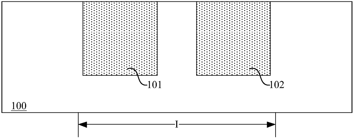
[0021] Please refer to figure 1 , providing a substrate 100 including a high voltage region I of peripheral circuits.

[0022] The substrate 100 can be a semiconductor material, such as a single crystal silicon substrate, a single crystal germanium substrate, SOI (silicon on insulator) or GOI (germanium on insulator) substrate, etc., and the substrate 100 can also be a P Type doping or N type doping. A person skilled in the art can select a suitable material as the substrate according to actual requirements, which is not limited herein.

[0023] The substrate 100 is used to form a memory, including a storage area and a peripheral circuit area, and the peripheral circuit area is used to form a peripheral circuit to control the memory cells in th...


PUM

PropertyMeasurementUnit
Doping concentrationaaaaaaaaaa

Abstract

The present invention relates to a forming method of a threshold adjustment layer of a memory peripheral circuit, and a peripheral circuit structure. The forming method of the threshold adjustment layer comprises the following steps of providing a substrate, wherein the substrate comprises a high voltage region of a peripheral circuit; forming a patterned mask layer on the surface of the substrate, wherein the patterned mask layer exposes at least a portion of the high voltage region; using the patterned mask layer as a mask to perform threshold adjustment injection on the high voltage region,wherein a threshold adjustment layer is formed in the high voltage region and / or a gate dielectric layer of a high voltage device is formed on the surface of the high voltage region. The threshold adjustment layer is formed only in the high voltage region to avoid the performance of other regional devices from being affected.

Description

technical field [0001] The invention relates to the field of semiconductor technology, in particular to a method for forming a threshold adjustment layer of a memory peripheral circuit and a peripheral circuit structure. Background technique [0002] In recent years, the development of flash memory (Flash Memory) is particularly rapid. The main feature of flash memory is that it can keep stored information for a long time without power on, and has the advantages of high integration, fast access speed, easy erasing and rewriting, etc. Has been widely used. [0003] In the semiconductor process, especially the forming process of the memory, due to cost considerations, reducing the number of photomasks is a very important issue, and it is necessary to reduce the number of photomasks and process steps as much as possible. [0004] In the formation process of the flash memory, it is necessary to perform threshold adjustment implantation in the high-voltage device area of ​​the ...

Claims


Application Information

Patent Timeline
IPC IPC(8): H01L27/11526H01L27/11573
CPCH10B41/40H10B43/40
Inventor 许文山田武
Owner YANGTZE MEMORY TECH CO LTD
Features
  • R&D
  • Intellectual Property
  • Life Sciences
  • Materials
  • Tech Scout
  • Unparalleled Data Quality
  • Higher Quality Content
  • 60% Fewer Hallucinations
Learn More