Optical processing system of perovskite single crystal and application of perovskite single crystal with remarkably enhanced fluorescence

An optical processing and perovskite technology, applied in metal processing equipment, manufacturing tools, laser welding equipment, etc., can solve problems such as imperfect processing, large stress, damage, etc., to achieve a wide range of effects

Inactive Publication Date: 2018-09-14
CHANGCHUN INST OF OPTICS FINE MECHANICS & PHYSICS CHINESE ACAD OF SCI
View PDF5 Cites 5 Cited by
  • Summary
  • Abstract
  • Description
  • Claims
  • Application Information

AI Technical Summary

Problems solved by technology

However, these technologies inevitably contain dangerous chemical solutions in the actual processing process, and direct contact with the processed samples will generate greater stress, which will lead to MAPbBr 3 Degradation, destruction and imperfect handling of single crystals

Method used


Image

  • Optical processing system of perovskite single crystal and application of perovskite single crystal with remarkably enhanced fluorescence
  • Optical processing system of perovskite single crystal and application of perovskite single crystal with remarkably enhanced fluorescence
  • Optical processing system of perovskite single crystal and application of perovskite single crystal with remarkably enhanced fluorescence

Examples


Embodiment Construction

[0028] The following will clearly and completely describe the technical solutions in the embodiments of the present invention with reference to the accompanying drawings in the embodiments of the present invention. Obviously, the described embodiments are only some, not all, embodiments of the present invention. Based on the embodiments of the present invention, all other embodiments obtained by persons of ordinary skill in the art without making creative efforts belong to the protection scope of the present invention.

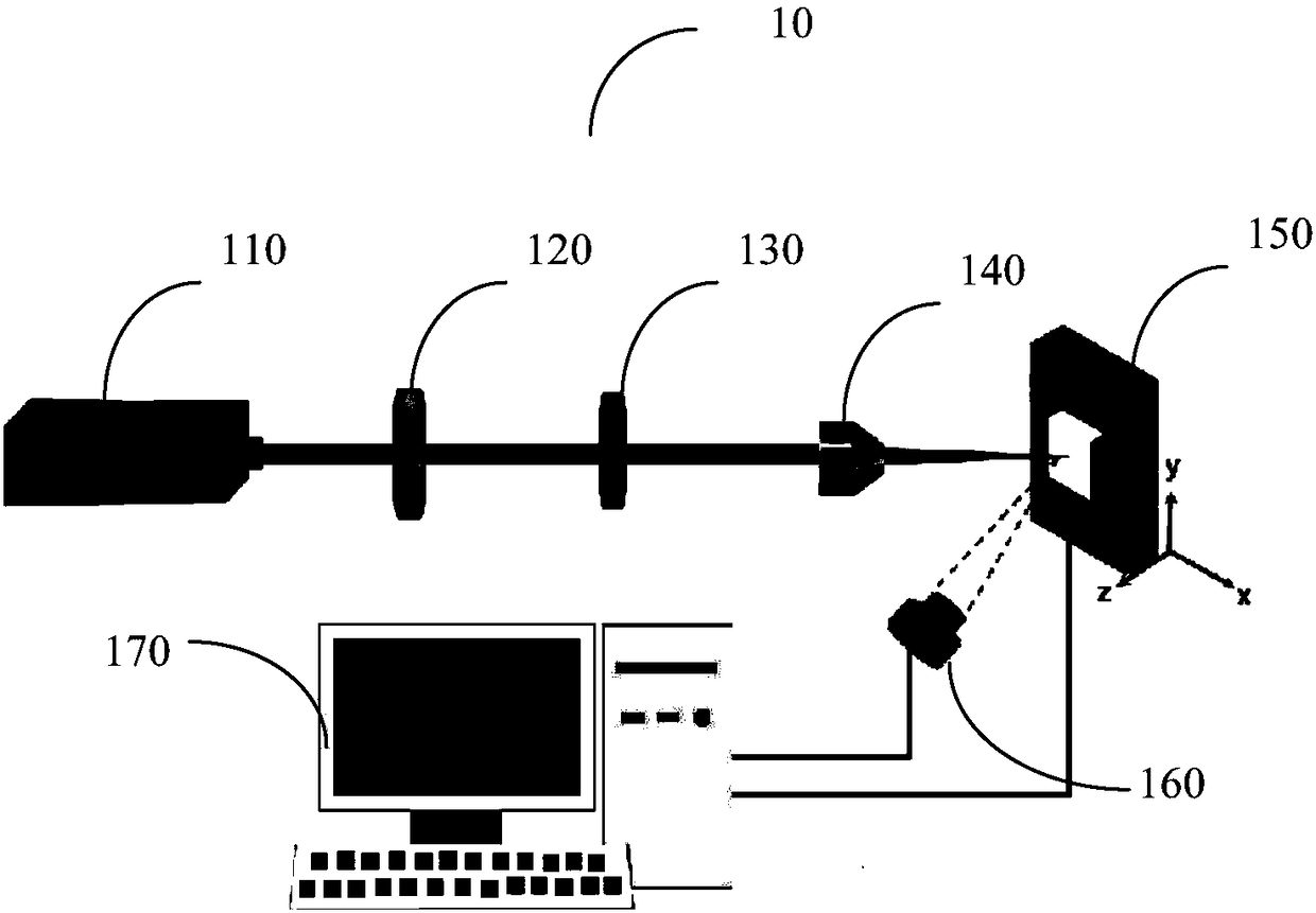
[0029] see figure 1 , is a schematic structural diagram of an optical processing system 10 for a perovskite single crystal provided in an embodiment of the present invention, including: a laser light source 110, a numerical aperture 120, an attenuator 130, an objective lens 140, a three-dimensional translation stage 150, a charge-coupled device 160 and a computer 170 , the three-dimensional translation stage 150 is provided with a perovskite single crystal, an...


PUM


Abstract

The invention discloses an optical processing system of perovskite single crystal. The system comprises a laser light source, a numerical aperture, an attenuator, an objective lens, a three-dimensional translation table, a charge coupling device and a computer; a femtosecond laser light beam emitted by a femtosecond laser light source sequentially passes through the numerical aperture, the attenuator and the objective lens and then is focused on the surface of the perovskite single crystal on a three-dimensional translation table, and micro-machining on the surface of the perovskite single crystal is carried out to obtain the perovskite single crystal with remarkably enhanced fluorescence; and a charge coupling device can transmit the micro-machining process to a computer. According to thesystem, the optical processing system of the perovskite single crystal is used for realizing induction etching of various morphologies of the surface of the perovskite single crystal by controlling relevant laser processing parameters; and based on that the surface trap density of the perovskite single crystal is reduced and the principle of changing the surface state of the perovskite single crystal, the remarkable enhancement of the fluorescence property is realized.

Description

technical field [0001] The invention relates to the technical field of laser processing, in particular to an optical processing system and application of a perovskite single crystal. Background technique [0002] Due to the unique crystal structure of perovskite AMX 3 (A=organic or inorganic cation, M=metal cation and X=halogen anion), which make it have excellent photoelectric properties and have been applied in solar cells, light-emitting diodes (LEDs), lasers, field-effect transistors and photodetectors and other optoelectronic devices. [0003] So far, the most widely used perovskite morphologies can be classified into polycrystalline films, nanowires, nanosheets, nanorods, quantum dots, bulk single crystals, and other morphologies. Among all morphologies, bulk single crystals have better charge transfer and transport properties than other morphologies due to fewer traps and grain boundaries. For example, MAPbI has been reported 3 The carrier diffusion length in sing...

Claims


Application Information

Patent Timeline
IPC IPC(8): B23K26/362B23K26/402B23K26/12
CPCB23K26/123B23K26/361B23K26/402
Inventor 于伟利邢军郭春雷
Owner CHANGCHUN INST OF OPTICS FINE MECHANICS & PHYSICS CHINESE ACAD OF SCI
Why Eureka
Try Eureka