Manufacturing method of packaging substrate

A technology for encapsulating substrates and manufacturing methods, applied in semiconductor/solid-state device manufacturing, electrical components, electrical solid-state devices, etc., can solve problems such as low output efficiency, difficulty in providing, and high requirements for machine thin plate capabilities, and achieve fine layout , the effect of improving output efficiency

Active Publication Date: 2018-09-18
ASE SHANGHAI
View PDF5 Cites 1 Cited by
  • Summary
  • Abstract
  • Description
  • Claims
  • Application Information

AI Technical Summary

Problems solved by technology

Because the dielectric material layer is very thin, it is difficult to provide sufficient support during the manufacturing process. Therefore, the traditional technology usually divides the lines on the upper and lower sides of the dielectric material layer into two parts. However, this process can only produce one substrate at a time, and the output efficiency is low.
Moreover, because the thickness of the packaging substrate to be manufactured is relatively thin, the traditional technology also requires high thin plate capability of the machine.

Method used


Image

  • Manufacturing method of packaging substrate
  • Manufacturing method of packaging substrate
  • Manufacturing method of packaging substrate

Examples


Embodiment Construction

[0013] In order to better understand the spirit of the present invention, it will be further described below in conjunction with some preferred embodiments of the present invention.

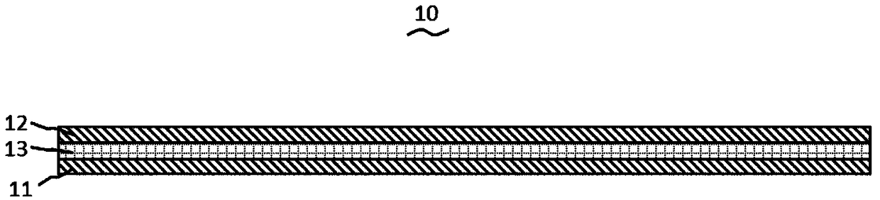
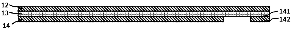
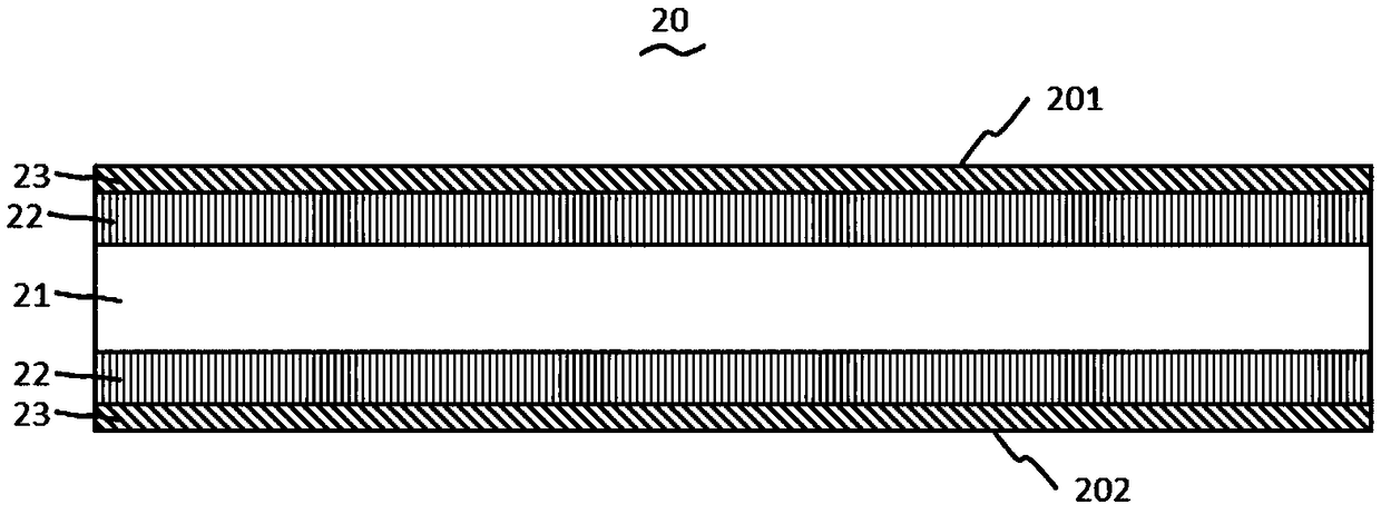
[0014] Figure 1-11 Shown is a schematic cross-sectional view of the packaging substrate in different manufacturing stages of the manufacturing process of the packaging substrate according to an embodiment of the present invention. However, those skilled in the art can fully understand based on the examples of the embodiments of the present invention Figure 11 The package substrate 100 shown can also be obtained according to other embodiments of the present invention, and is not limited to Figure 1-10 The illustrated steps. In other words, what those skilled in the art can determine based on the following disclosure is that the manufacturing process of the packaging substrate should be adjusted accordingly due to the structure or production requirements of the packaging substrate. This embodim...


PUM

PropertyMeasurementUnit
thicknessaaaaaaaaaa
thicknessaaaaaaaaaa

Abstract

The invention relates to a manufacturing method of a packaging substrate. According to the embodiment of the invention, the manufacturing method comprises steps of providing an overlapping structure,wherein the first overlapping structure comprises a first metal layer, a second metal layer and a capacitance medium layer arranged between the first metal layer and the second metal layer; carrying out patterning processing on the first metal layer of the first overlapping structure so as to form a first circuit layer; providing a carrier plate, wherein the carrier plate comprises a first surfaceand a second surface, and the first surface is opposite to the second surface; laminating a first dielectric layer and the first overlapping structure subjected to the patterning processing on the first surface and the second surface of the carrier plate; and carrying out patterning processing on the first surface and the second surface so as to form a second circuit layer. According to the invention, precise layout of inner elements of the packaging substrate is achieved; and yield efficiency of the packaging substrate is improved.

Description

technical field [0001] The invention relates to the technical field of semiconductors, in particular to a method for manufacturing a packaging substrate. Background technique [0002] In the current semiconductor packaging technology, placing capacitive elements inside the packaging substrate is a solution to realize the miniaturization of electronic systems. This solution is usually used in electronic products such as microphones and wearable devices, which can play a role in filtering, timing, Decoupling and the role of electrical energy storage. In this way, not only the stability and reliability of the product can be improved, but also the physical size of the product can be reduced. [0003] The capacitive element generally consists of two layers of copper foil with a thickness of 35 μm or 70 μm and a dielectric material layer with a thickness of 20 μm or less between the two layers of copper foil. Because the dielectric material layer is very thin, it is difficult to...

Claims


Application Information

Patent Timeline
Patent Type & Authority Applications(China)
IPC IPC(8): H01L21/60
CPCH01L24/27
Inventor 欧宪勋程晓玲韩建华
Owner ASE SHANGHAI
Why Eureka
Try Eureka