Semiconductor structure and forming method thereof

A semiconductor and gate structure technology, which is applied in semiconductor devices, semiconductor/solid-state device manufacturing, semiconductor/solid-state device components, etc., can solve the problem that the surface of the wafer cannot provide enough area interconnection lines, etc., to reduce metal-induced Effects of gap state phenomenon, performance improvement, and contact resistance reduction

Active Publication Date: 2018-09-25
SEMICON MFG INT (SHANGHAI) CORP +1
View PDF4 Cites 1 Cited by
  • Summary
  • Abstract
  • Description
  • Claims
  • Application Information

AI Technical Summary

Problems solved by technology

In order to improve integration and reduce costs, the critical dimensions of components are getting smaller and the circuit density inside integrated circuits is inc

Method used


Image

  • Semiconductor structure and forming method thereof
  • Semiconductor structure and forming method thereof
  • Semiconductor structure and forming method thereof

Examples


Embodiment Construction

[0034] It can be seen from the background art that there is a problem of excessive contact resistance in the semiconductor structure with plugs introduced in the prior art. Combining with a method of forming a semiconductor structure, the reason for the excessive contact resistance is analyzed:

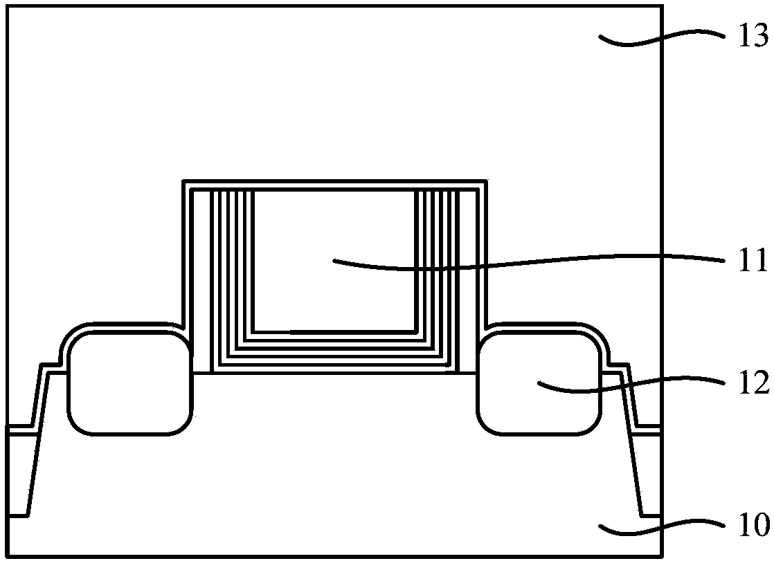
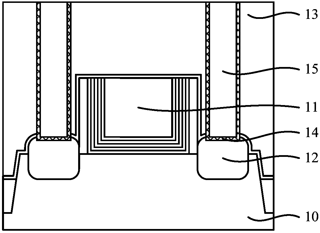
[0035] refer to figure 1 and figure 2 , shows a schematic cross-sectional structure corresponding to each step of a method for forming a semiconductor structure.

[0036] Such as figure 1 As shown, a substrate 10 is provided; a gate structure 11 located on the substrate 10 is formed; a stress layer 12 located on both sides of the gate structure is formed, and the stress layer 12 is doped to form a source and drain A doped region: a dielectric layer 13 is formed on the substrate 10 exposed by the gate structure 11 , and the dielectric layer 13 covers the stress layer 12 .

[0037] Such as figure 2 As shown, a plug 15 is formed in the dielectric layer 13 on the stress layer 12 , ...


PUM

PropertyMeasurementUnit
Thicknessaaaaaaaaaa

Abstract

Disclosed are a semiconductor structure and a forming method thereof. The forming method includes the following steps: forming a substrate; forming a gate structure on the substrate; forming source-drain doping regions located in the substrate on two sides of the gate structure; forming a dielectric layer on the substrate exposing from the gate structure, wherein the dielectric layer covers the source-drain doping regions; forming contacting holes passing through the dielectric layer, wherein the bottoms of the contacting holes expose the source-drain doping regions; forming an oxide metal layer on the source-drain doping regions exposing from the contacting holes; and forming plugs in the contacting holes in which the oxide metal layer is formed. The technical scheme of the invention caneffectively inhibit the phenomenon of Fermi level pinning at the interface of the plugs and the source-drain doping regions, thereby benefiting the reduction of the contact resistance between the plugs and the source-drain doping regions, and benefiting the improvement of the performance of the formed semiconductor structure.

Description

technical field [0001] The invention relates to the field of semiconductor manufacturing, in particular to a semiconductor structure and a forming method thereof. Background technique [0002] In the integrated circuit manufacturing process, after the semiconductor device structure is formed, it is necessary to connect the semiconductor devices together to form a circuit. With the continuous development of integrated circuit manufacturing technology, people's requirements for the integration and performance of integrated circuits are becoming higher and higher. In order to improve integration and reduce costs, the critical dimensions of components are getting smaller and the circuit density inside integrated circuits is increasing. This development makes it impossible for the surface of the wafer to provide enough area to make the interconnection lines required by conventional circuits. . [0003] In order to meet the requirements of the interconnection line after the crit...

Claims


Application Information

Patent Timeline
IPC IPC(8): H01L21/768H01L23/532H01L23/535H01L21/336H01L29/78
CPCH01L21/76847H01L21/76877H01L21/76895H01L23/53257H01L23/535H01L29/66795H01L29/785H01L2029/7858H01L2221/1073
Inventor 周飞
Owner SEMICON MFG INT (SHANGHAI) CORP
Why Eureka
Try Eureka