Formation method of semiconductor structure

A semiconductor and gas technology, used in semiconductor/solid-state device manufacturing, electrical components, circuits, etc., to solve the problem that the threshold voltage of transistors is difficult to meet design requirements

Active Publication Date: 2021-03-09
SEMICON MFG INT (SHANGHAI) CORP +1
View PDF5 Cites 0 Cited by
  • Summary
  • Abstract
  • Description
  • Claims
  • Application Information

AI Technical Summary

Problems solved by technology

[0004] However, the threshold voltage of the transistor formed by the prior art is difficult to meet the design requirements

Method used


Image

  • Formation method of semiconductor structure
  • Formation method of semiconductor structure
  • Formation method of semiconductor structure

Examples


Embodiment Construction

[0025] As mentioned in the background, the threshold voltage of the semiconductor structure formed in the prior art is difficult to meet the design requirements.

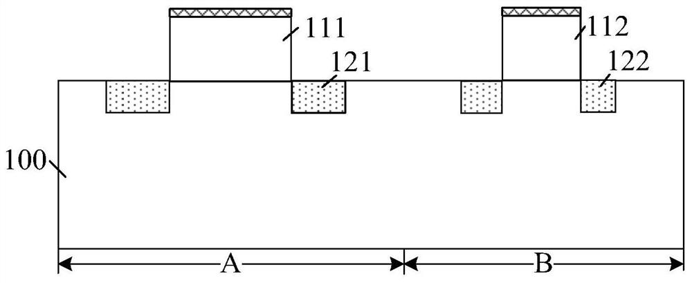
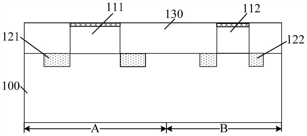
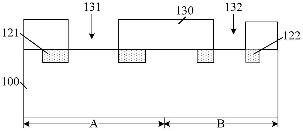
[0026] The method for forming a semiconductor structure includes: providing a substrate with a dielectric layer on the substrate, an opening in the dielectric layer, and the opening passing through the dielectric layer; forming a gate dielectric layer at the bottom of the opening; A work function layer is formed on the gate dielectric layer; after the work function layer is formed, a gate is formed in the opening.

[0027] Wherein, the semiconductor structure is an NMOS transistor, and the work function layer is titanium aluminum. The work function layer is used to reduce the threshold voltage of the formed semiconductor structure, and the precursor for forming the work function layer is a carbon-containing precursor. In the process of forming the work function layer, carbon atoms in the precursor inevitably enter ...


PUM


Abstract

A method for forming a semiconductor structure, comprising: providing a substrate; forming a work function layer on the substrate, the step of forming the work function layer includes one or more steps of forming a work function film, and the step of forming the work function film includes: An initial work function film is formed on the substrate, and the initial work function film has carbon atoms; the carbon removal precursor is used to remove carbon from the initial work function film to form a work function film, and the carbon removal precursor is used to interact with The carbon atoms in the initial work function film react; a gate is formed on the work function layer. A gate is formed on the work function layer. After the initial work function film is formed, the carbon removal treatment is performed on the initial work function film through the carbon removal precursor. The carbon-removing precursor can react with the carbon atoms in the initial work function film, thereby reducing the carbon atom content in the initial work function film, thereby changing the work function of the work function layer, and then adjusting the threshold voltage of the formed transistor, so that all The threshold voltage of the formed transistor meets the design requirements.

Description

technical field [0001] The invention relates to the field of semiconductor manufacturing, in particular to a method for forming a semiconductor structure. Background technique [0002] With the continuous progress of semiconductor technology, the integration level of semiconductor devices has been continuously improved, which requires that more transistors can be formed on a chip. [0003] Threshold voltage is an important parameter of transistors, which has a great influence on the performance of transistors. Transistors with different functions often have different requirements on threshold voltages. During the process of forming different transistors, the threshold voltages of different transistors need to be adjusted. In order to adjust the threshold voltages of different transistors, a work function layer is often formed on the surface of the gate dielectric layer of the transistor. Transistors can have different threshold voltages by selecting the thickness and mater...

Claims


Application Information

Patent Timeline
Patent Type & Authority Patents(China)
IPC IPC(8): H01L21/8234
CPCH01L21/823462
Inventor 邓浩徐建华
Owner SEMICON MFG INT (SHANGHAI) CORP
Why Eureka
Try Eureka