Method for loading primary polycrystalline silicon material and reclaimed material in production of casting monocrystals

A technology of polysilicon and recycled materials, which is applied in the directions of single crystal growth, single crystal growth, polycrystalline material growth, etc., can solve the problem of less research on the charging methods of primary polysilicon materials and recycled materials, and less research on the laying method of single crystal seed layer. Many problems, to achieve the effect of reducing production costs, reducing the risk of rupture, and reducing the outflow of silicon liquid

Inactive Publication Date: 2018-10-02
JIANGXI SORNID HI TECH
View PDF0 Cites 10 Cited by
  • Summary
  • Abstract
  • Description
  • Claims
  • Application Information

AI Technical Summary

Problems solved by technology

[0006] The purpose of the present invention is to provide a method for charging primary polysilicon material and reclaimed material when producing cast single crystal, which solves the problem that the existing primary polycrystalline silicon material and rec...

Method used


Image

  • Method for loading primary polycrystalline silicon material and reclaimed material in production of casting monocrystals
  • Method for loading primary polycrystalline silicon material and reclaimed material in production of casting monocrystals
  • Method for loading primary polycrystalline silicon material and reclaimed material in production of casting monocrystals

Examples


Embodiment 1

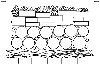
[0044] A kind of charging method of native polysilicon material and reclaimed silicon material, such as figure 1 shown, including the following steps:

[0045] In step a, a plurality of single crystal seed crystals in the shape of small cuboids are tightly laid on the bottom of the crucible G5 to form a complete single crystal seed layer, and a complete single crystal seed layer consists of 36 small cuboid single crystals Seed crystal composition, the size of the small cuboid single crystal seed crystal is 125mm×125mm×20mm.

[0046] In step b, polysilicon fragments are spread on the silicon wafer, and the thickness of the fragmented silicon wafer is 60 mm.

[0047] In step c, the side skins of four polysilicon ingots are closely attached to each side wall of the crucible, leaving a distance of 3 mm between the two side skins.

[0048] In step d, two layers of primary dense rods are stacked on the polysilicon fragments, and the primary dense rods lean against the edge skins o...

Embodiment 2

[0054] In the production of cast single crystal, a charging method of primary polysilicon material and recycled silicon material, such asfigure 1 shown, including the following steps:

[0055] Step a: Lay multiple small cuboid-shaped single crystal seed crystals closely on the bottom of the crucible G6 to form a complete single crystal seed crystal layer, and a complete single crystal seed crystal layer consists of 36 small cuboid-shaped single crystal crystals Seed crystal composition, the size of the small cuboid single crystal seed crystal is 156mm×156mm×20mm.

[0056] In step b, polysilicon fragments are spread on the silicon wafer, and the thickness of the fragmented silicon wafer is 80 mm.

[0057] In step c, the side skins of 5 polysilicon ingots are closely attached to each side wall of the crucible, leaving a distance of 4 mm between the two side skins.

[0058] In step d, two layers of primary dense rods are stacked on the polysilicon fragments, and the primary dens...


PUM

PropertyMeasurementUnit
Thicknessaaaaaaaaaa
Thicknessaaaaaaaaaa

Abstract

The invention provides a method for loading a primary polycrystalline silicon material and a reclaimed material in production of casting monocrystals. The method comprises the following step: layers of monocrystal seeds, broken silicon slices, flaw-pieces, primary dense bar stocks or a large cauliflower-like material, small primary silicon material, the reclaimed material and a small reclaimed material are laid from the bottom of a crucible in sequence. The method has characteristics as follows: by means of the broken silicon slices, stress concentration above a seed crystal layer is avoided,thermal shock of a silicon liquid to the seed crystal layer at a melting stage is reduced, and dislocation caused by the stress concentration and thermal stress is reduced; the primary silicon material is laid at the lower part of the crucible, the reclaimed material is laid at the upper part of the crucible, and dislocation and polycrystals produced by impurity gathering at the initial seeding stage are reduced; a flaw-piece layer is tightly attached to the wall of the crucible, so that falling of a coating can be reduced, the adjacent flaw-pieces are spaced with certain distance, the flaw-pieces are prevented from expanding and extruding the crucible at high temperature, and the risk of crucible breakage can be reduced.

Description

technical field [0001] The invention relates to a method for charging primary polysilicon material and recycled material when producing cast single crystal. Background technique [0002] Crystalline silicon occupies an absolute advantage in the current solar energy material market. In terms of its crystal form, it can be divided into three categories: amorphous silicon, monocrystalline silicon, and polycrystalline silicon. The cost of amorphous silicon cells is low, but the conversion efficiency is also low, and due to the light-induced attenuation effect of amorphous silicon, its performance stability is poor; the content of impurities and defects in monocrystalline silicon cells is low, and the conversion efficiency is high, but The preparation process is complicated, and the purity of raw materials is high, so the production cost is also high; the production cost of polycrystalline silicon cells is low, but there are a large number of grain boundaries, high-density disloc...

Claims


Application Information

Patent Timeline
IPC IPC(8): C30B11/02C30B11/14C30B29/06
CPCC30B11/02C30B11/14C30B29/06
Inventor 张泽兴刘世龙黄林雷琦刘超王超徐云飞姚晨赖昌权
Owner JIANGXI SORNID HI TECH
Why Eureka
Try Eureka