Display panel and display apparatus

A display panel and substrate technology, applied in organic semiconductor devices, electrical components, electric solid devices, etc., can solve the problem of low photon density, achieve the effects of improving luminous efficiency, increasing spontaneous radiation rate, and increasing light extraction rate

Active Publication Date: 2018-10-02
WUHAN CHINA STAR OPTOELECTRONICS SEMICON DISPLAY TECH CO LTD
View PDF1 Cites 20 Cited by
  • Summary
  • Abstract
  • Description
  • Claims
  • Application Information

AI Technical Summary

Problems solved by technology

[0020] The invention provides a display panel display device to solve t

Method used


Image

  • Display panel and display apparatus
  • Display panel and display apparatus
  • Display panel and display apparatus

Examples


Embodiment Construction

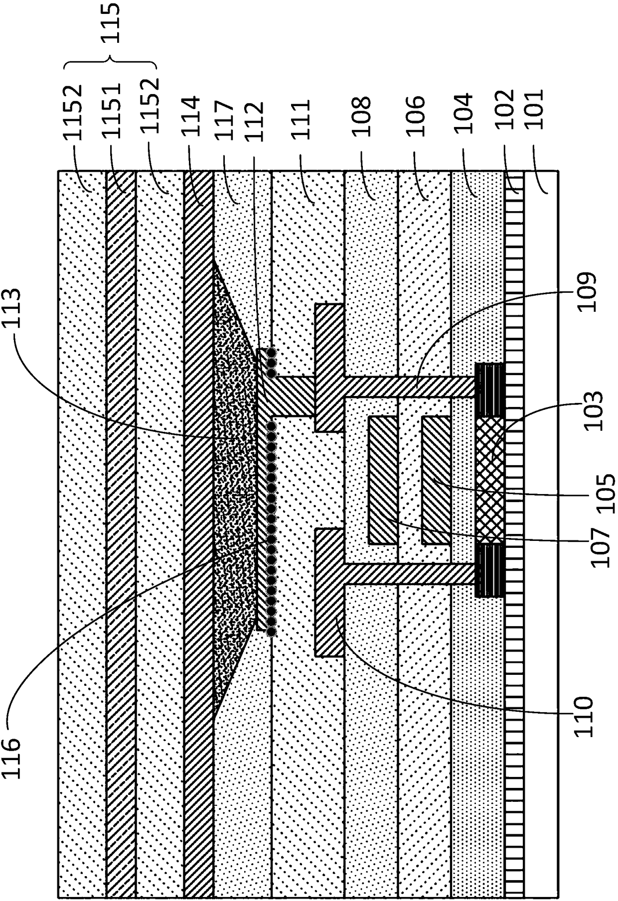
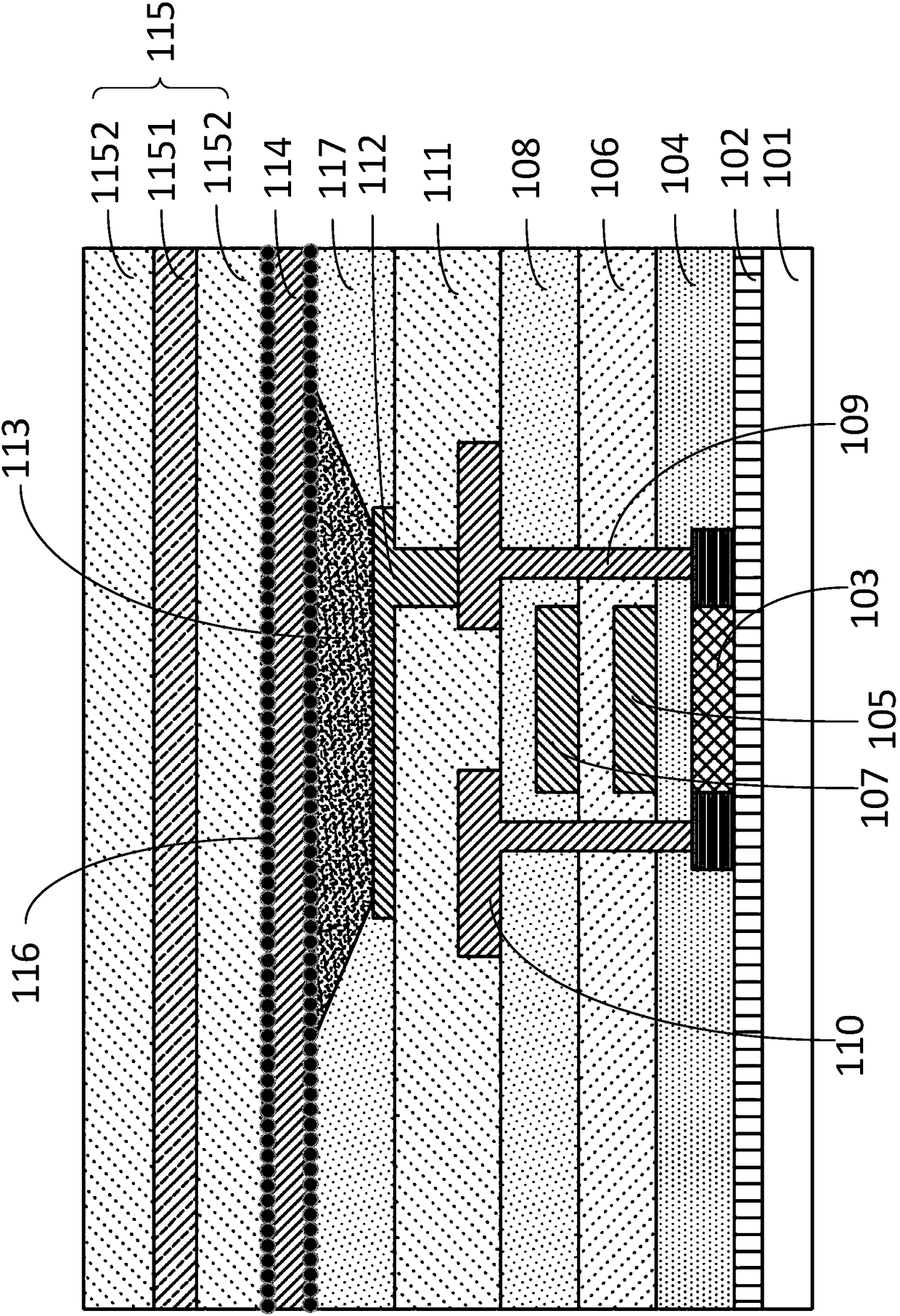
[0057] The following descriptions of the various embodiments refer to the accompanying drawings to illustrate specific embodiments in which the invention may be practiced. The directional terms mentioned in the present invention, such as [top], [bottom], [front], [back], [left], [right], [inside], [outside], [side], etc., are only for reference The orientation of the attached schema. Therefore, the directional terms used are used to illustrate and understand the present invention, but not to limit the present invention. In the figures, structurally similar elements are denoted by the same reference numerals.

[0058] figure 1 It is a film layer structure diagram of a display panel according to a preferred embodiment of the present invention. The display panel includes a substrate, a thin film transistor layer, an anode layer, an OLED layer, a cathode layer, a thin film encapsulation layer and a particle layer.

[0059] Substrate, the raw material of the substrate 101 may be...


PUM


Abstract

The invention provides a display panel and a display apparatus. The display panel comprises a substrate, a thin film transistor layer, a positive electrode layer, an organic light emitting layer, a negative electrode layer, a thin film packaging layer and a particle layer. According to the display panel, the particle layer is arranged between the thin film transistor layer and the thin film packaging layer; the particle layer consists of multiple silver nanoparticles; equivalently, photon state density and exciton spontaneous radiation efficiency are improved according to an SPR effect on surfaces of the nanoparticles, so as to improve the luminous efficiency of an AMOLED display panel; and in addition, by virtue of a light reflection effect of the silver nanoparticle layer, loss of lightrays can be reduced, and the light extracting efficiency of the AMOLED is improved.

Description

technical field [0001] The invention relates to the display field, in particular to a display panel display device. Background technique [0002] In flat panel display technology, Organic Light-Emitting Diode (OLED) display has many advantages such as thinness, active light emission, fast response speed, large viewing angle, wide color gamut, high brightness and low power consumption, etc., and has gradually become the successor. The third generation display technology after liquid crystal display. Compared with LCD (Liquid crystal displays, liquid crystal display), OLED has the advantages of saving power, being thinner, and having a wider viewing angle, which is incomparable to LCD. At present, people have higher and higher requirements for the fineness of the display, that is, the resolution, but the production of high-quality, high-resolution OLED displays still faces many challenges. [0003] According to the driving method, OLED display devices can be divided into two...

Claims


Application Information

Patent Timeline
IPC IPC(8): H01L27/32H01L51/52
CPCH10K59/12H10K50/85H10K50/856H10K2102/331H10K50/84H10K59/122H10K59/1201
Inventor 万凯钟小华
Owner WUHAN CHINA STAR OPTOELECTRONICS SEMICON DISPLAY TECH CO LTD
Why Eureka
Try Eureka