
High-efficiency lasing output dfb semiconductor laser device and photonic integrated emission chip

A laser and semiconductor technology, applied in the field of optoelectronics, can solve problems such as unbalanced laser power, unbalanced output laser power of laser arrays, abnormally complex structure of laser arrays, etc., and achieve the effects of laser self-feedback enhancement, shortened length, and reduced threshold current

Active Publication Date: 2020-09-01
CHANGZHOU INST OF TECH
View PDF2 Cites 0 Cited by
  • Summary
  • Abstract
  • Description
  • Claims
  • Application Information

AI Technical Summary

Problems solved by technology

The disadvantage of using this method is that it will lead to unbalanced output laser power of the laser array
Using electrothermal devices or changing the injection current to adjust the lasing wavelength to align with the ITU-T standard will not only cause a serious imbalance in the output laser power of each unit laser, but also cause an extremely complex structure of the laser array

Method used


Image

  • High-efficiency lasing output dfb semiconductor laser device and photonic integrated emission chip
  • High-efficiency lasing output dfb semiconductor laser device and photonic integrated emission chip
  • High-efficiency lasing output dfb semiconductor laser device and photonic integrated emission chip

Examples


Embodiment 1

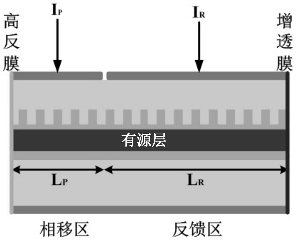
[0026] This embodiment provides a high-efficiency lasing output DFB semiconductor laser device, such as figure 1 As shown, the frequency selection grating is a uniform grating or a uniform sampling grating. The whole laser is divided into two parts: a phase shift area and a feedback area. Other anti-reflection measures.

[0027] In this embodiment: the electrodes in the phase shift region and the feedback region can be electrically isolated by a certain distance, or by implanting helium ions, or by etching an electrical isolation trench.

[0028] The realization principle of the fine adjustment of the lasing wavelength of the high-efficiency lasing output DFB semiconductor laser device of the present invention is as follows:

[0029] we take figure 1 As an example to illustrate, for the sake of simplicity, the lengths of the feedback region and the phase shift region of the laser are respectively L P =L, then when the feedback region and the phase shift region of the lase...

Embodiment 2

[0039] This embodiment provides a distributed feedback semiconductor laser monolithic integrated array, which is composed of the high-efficiency lasing output DFB semiconductor laser device described in the first embodiment.

[0040] This embodiment also provides a photonic integrated emission chip (such as Figure 4 shown), the module consists of a laser monitor array, the above-mentioned distributed feedback semiconductor laser monolithic integrated array, a modulator array, a power equalizer array and a multiplexer, which are sequentially grown and integrated into formed on the same epitaxial wafer.

Embodiment 3

[0042] This embodiment adopts a manufacturing method of a distributed feedback semiconductor laser and an array thereof, the steps of which are as follows:

[0043] (1) Epitaxial n-type InP buffer layer, 100nm thick undoped lattice-matched InGaAsP lower confinement layer, strained InGaAsP multiple quantum wells and 100nm thick p-type lattice-matched InGaAsP upper confinement layer on n-type InP substrate material Floor;

[0044] (2) The production method of the grating:

[0045] ① Manufacturing method of uniform grating: use the method of double-beam holographic interference exposure to record the uniform grating pattern on the photoresist on the upper confinement layer, and then apply material etching to form the required uniform grating on the upper part of the upper confinement layer structure. figure 2 It is a schematic diagram of the process of making a uniform grating by double ultraviolet beam interference.

[0046] ②Uniform sampling grating manufacturing method, us...


PUM

PropertyMeasurementUnit
reflectanceaaaaaaaaaa

Abstract

The invention discloses a high-efficiency lasing output DFB semiconductor laser device and a photon integrated transmitting chip. The frequency selective grating of the laser device is a common uniform grating or a uniform sampling grating that has two electrodes electrically isolated from each other, one end surface of the laser is plated with a high reflection film, and the other end face is coated with an antireflection film or adopts other light-emitting increasing measures. The invention improves the efficiency of the effective lasing output laser of the laser while reducing the thresholdof the laser. By changing the magnitude or proportion of the injection current in the phase shift region and the feedback region, the single mode lasing of the laser is continuously adjusted and thelasing wavelength meets the requirements of the ITU-T standard under the premise of eliminating the adverse effect of the end phase on the single mode of the laser. If the total operating current andthe operating temperature remain the same, the injection current ratio of the phase shift region and the feedback region of the laser is changed, so that the lasing output power of the laser may fluctuate very little when the single mode lasing of the laser is realized and the wavelength is continuously adjustable.

Description

technical field [0001] The invention belongs to the technical field of optoelectronics, and relates to optical fiber communication, photon integration, photoelectric sensing and other photoelectric information processing. The invention relates to a high-efficiency lasing output DFB semiconductor laser device with finely adjustable wavelength within a certain range and a manufacturing method thereof. Background technique [0002] As the core device of optical fiber communication system, distributed feedback (Distributed Feedback, DFB) semiconductor laser has attracted worldwide attention due to its small size and simple structure. In order to ensure the single-mode yield of DFB semiconductor lasers, it is usually necessary to introduce real phase shift or equivalent phase shift into its frequency-selective grating. In real phase-shift or equivalent phase-shift semiconductor lasers, in order to eliminate the lasing wavelength drift caused by various random factors, wavelength...

Claims


Application Information

Patent Timeline
Patent Type & Authority Patents(China)
IPC IPC(8): H01S5/12H01S5/40
CPCH01S5/1209H01S5/124H01S5/4025
Inventor 周亚亭赵勤贤
Owner CHANGZHOU INST OF TECH
Learn More