Phase shift mask blank and method for manufacturing phase shift mask using the same and pattern transfer method
A phase shift mask and manufacturing method technology, applied in the photoengraving process of the pattern surface, the original for photomechanical processing, optics, etc., can solve the problems of pattern position change, increase of thermal deformation of mask substrate, etc. , to achieve the effect of small CD deviation, good precision and good cross-sectional shape
- Summary
- Abstract
- Description
- Claims
- Application Information
AI Technical Summary
Problems solved by technology
Method used
Image
Examples
Embodiment approach 1
[0084] Embodiment 1 will describe a phase shift mask blank.
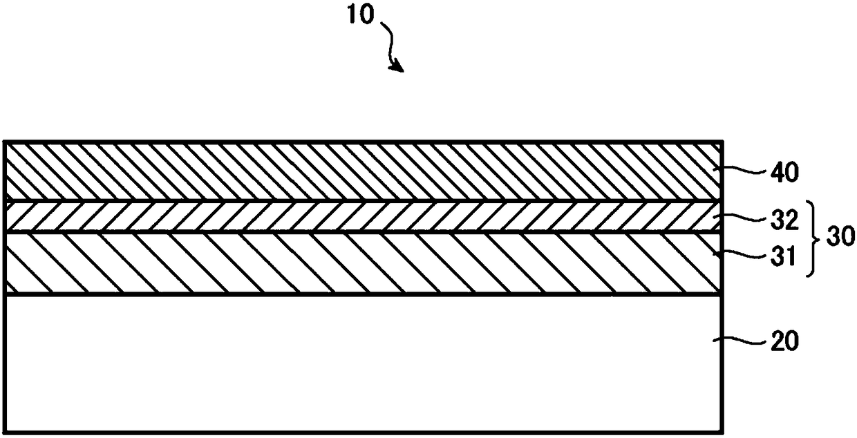
[0085] figure 1 It is a schematic diagram showing the film configuration of the phase shift mask blank 10 .
[0086] figure 1 The illustrated phase shift mask blank 10 has a transparent substrate 20 , a phase shift film 30 formed on the transparent substrate 20 , and a light shielding film 40 formed on the phase shift film 30 .
[0087] The transparent substrate 20 is transparent to exposure light. The transparent substrate 20 has a transmittance to exposure light of 85% or higher, preferably 90% or higher, when there is no surface reflection loss. The transparent substrate 20 is made of a material containing silicon and oxygen, and can be made of synthetic quartz glass, quartz glass, aluminosilicate glass, soda lime glass, low thermal expansion glass (SiO 2 -TiO 2 Glass, etc.) and other glass materials. When the transparent substrate 20 is made of low thermal expansion glass, it is possible to suppress the po...
Embodiment approach 2
[0146] In Embodiment 2, the manufacturing method of a phase shift mask is demonstrated.
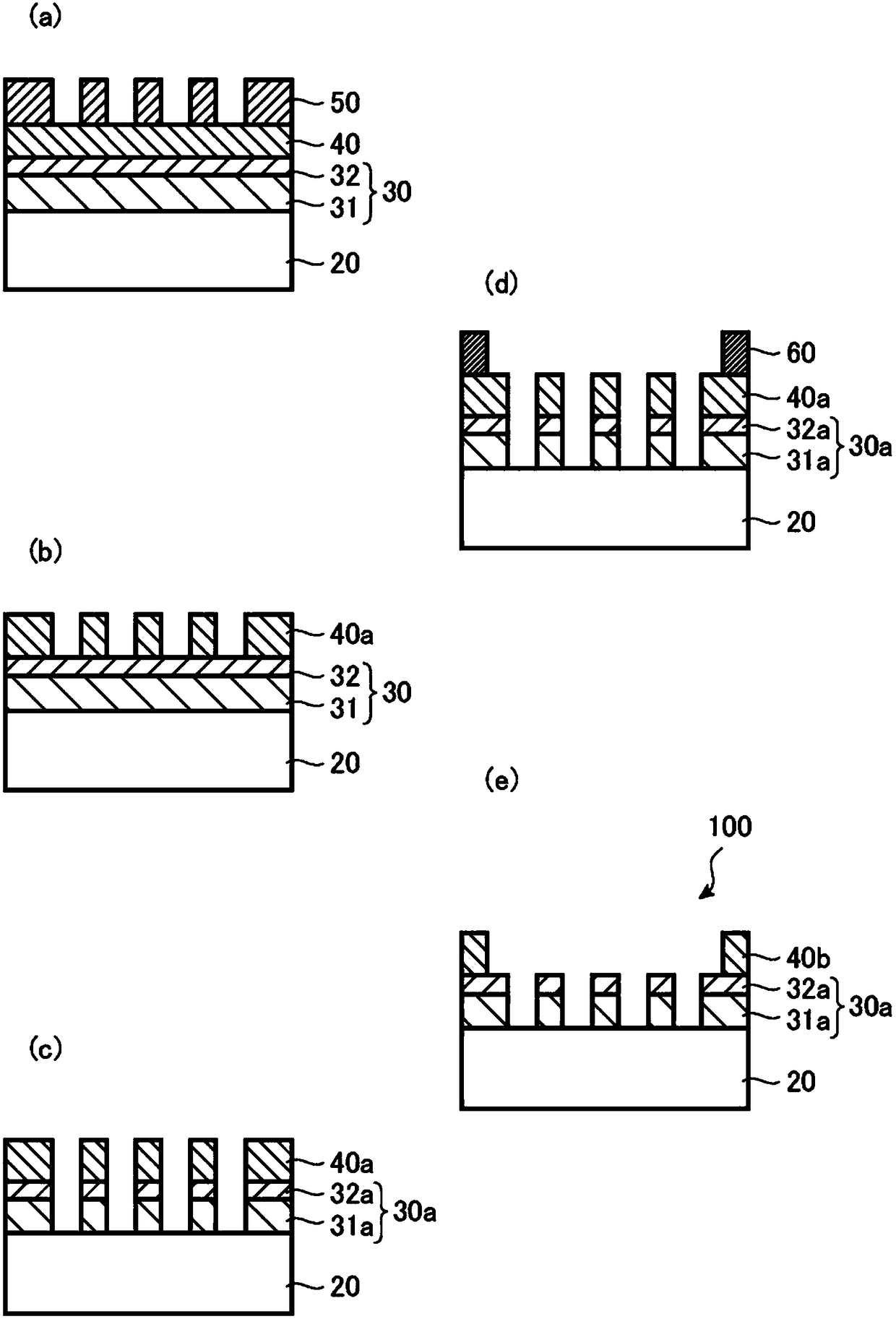
[0147] figure 2 is a schematic diagram illustrating a method of manufacturing a phase shift mask.
[0148] figure 2 The phase shift mask shown is fabricated using a figure 1 The manufacturing method of the phase shift mask blank of the phase shift mask blank 10 shown, this method comprises the following first resist pattern forming process, first light shielding film pattern forming process, phase shift film pattern forming process, second A resist pattern forming process, and a second light-shielding film pattern forming process.
[0149] Hereinafter, each step will be described in detail.
[0150] 1. First resist pattern formation process
[0151] In the first resist pattern forming step, first, a resist film is formed on the light shielding film 40 of the phase shift mask blank 10 according to the first embodiment. The material of the resist film to be used is not particularly ...
Embodiment approach 3
[0172] In Embodiment 3, a method of manufacturing a display device will be described. The display device was manufactured by performing the following mask placement step and pattern transfer step. The pattern transfer step corresponds to a pattern transfer method.
[0173] Hereinafter, each step will be described in detail.
[0174] 1. Loading process
[0175] In the mounting step, the phase shift mask manufactured in Embodiment 2 is mounted on the mask stage of the exposure apparatus. Here, the phase shift mask is arranged to face the resist film formed on the display device substrate via the projection optical system of the exposure device. For example, as the exposure apparatus, a projection exposure apparatus having an equal magnification projection optical system is used.
[0176] 2. Pattern transfer process
[0177] In the pattern transfer step, the phase shift mask is irradiated with exposure light to transfer the phase shift film pattern onto the resist film forme...
PUM
| Property | Measurement | Unit |
|---|---|---|
| thickness | aaaaa | aaaaa |
| thickness | aaaaa | aaaaa |
| thickness | aaaaa | aaaaa |
Abstract
Description
Claims
Application Information

