Integrated neural network for computational lithography

A neural network and computational lithography technology, applied in the field of integrated neural networks, can solve problems such as complex procedures, inability to guarantee efficiency, and time-consuming, and achieve the effects of reducing complexity, simple and fast process, and improving efficiency

Active Publication Date: 2018-10-16
SHANGHAI INTEGRATED CIRCUIT RES & DEV CENT
View PDF5 Cites 5 Cited by
  • Summary
  • Abstract
  • Description
  • Claims
  • Application Information

AI Technical Summary

Problems solved by technology

Therefore, the deep convolutional neural network architecture is complex in the process of computational

Method used


Image

  • Integrated neural network for computational lithography
  • Integrated neural network for computational lithography
  • Integrated neural network for computational lithography

Examples


Embodiment Construction

[0023] In order to make the purpose, technical solution and advantages of the present invention clearer, the specific implementation manners of the present invention will be further described in detail below in conjunction with the accompanying drawings.

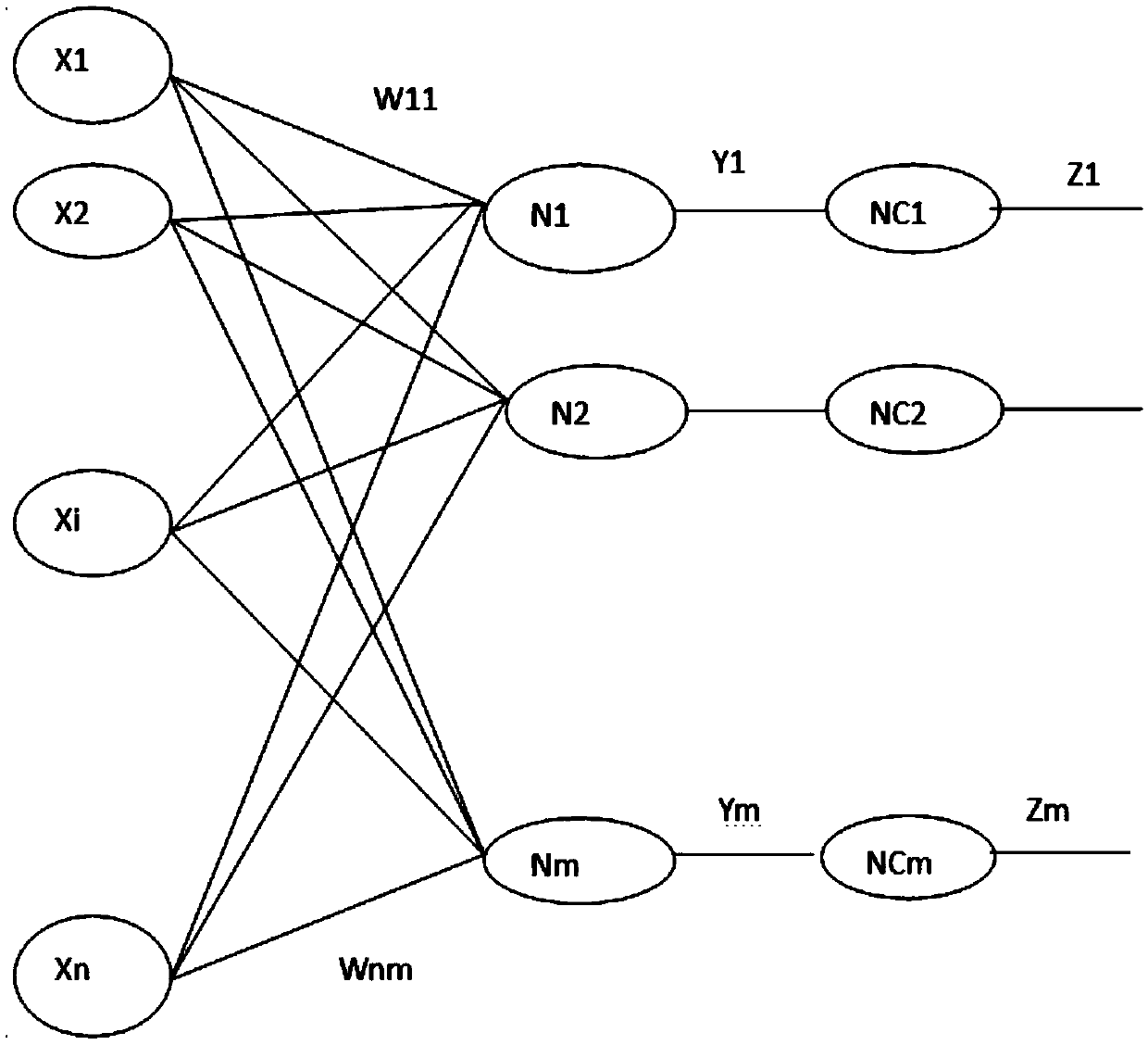
[0024] An integrated neural network for computing lithography provided by the present invention, the integrated neural network includes a conjugated neural network and a forward neural network, and the output of the conjugated neural network is connected to the input of the forward neural network; the conjugated neural network The network is used to extract the feature vector of computational lithography, and input the extracted feature vector into the forward neural network, wherein the method of extracting the feature vector of computational lithography by the conjugate neural network is: Y j =∑ i W ij x i , Among them, Z j is the extracted feature vector, W ij is the parameter of the conjugate neural network, X i i...


PUM


Abstract

Disclosed is an integrated neural network for computational lithography. The integrated neural network comprises a conjugate neural network and a feedforward neural network, and an output end of the conjugate neural network is connected with an input end of the feedforward neural network; the conjugate neural network is used for extracting a feature vector of the computational lithography and inputting the extracted feature vector to the feedforward neural network, wherein according to a method for using the conjugate neural network to extract the feature vector of the computational lithography, Yj is equal to sigmaiWijXi, and Zj is equal to the product of Yj and Yj*; Zj is the extracted feature vector, Wij is a parameter of the conjugate neural network, Xi is the adjacent environment of an i point on a photomask, and Yj* is the conjugation of Yj. According to the integrated neural network for the computational lithography, the conjugate convolutional neural network structure for extracting the feature vector and the feedforward neural network are combined to form the integrated neural network, and the integrated neural network can be used for various types of computational lithography learning.

Description

technical field [0001] The invention relates to the field of integrated circuits, in particular to an integrated neural network for computational lithography. Background technique [0002] In order to continuously pursue performance enhancement, power consumption reduction, and chip area shrinkage of semiconductor chips, the minimum feature pitch and minimum feature size of the semiconductor chip need to be reduced accordingly. To support this endless trend, the semiconductor industry needs to develop lithography tools, such as scanners, with increasingly shorter exposure wavelengths and higher numerical apertures (NA) to achieve high optical resolution. The semiconductor industry has successfully followed this path prior to the 14nm technology node, however, the industry has found it very difficult to continue to advance hardware (scanner) technology along this path. Development is slow to see. [0003] As a remedy, the development and application of computational lithogr...

Claims


Application Information

Patent Timeline
IPC IPC(8): G06N3/04G03F7/20
CPCG03F7/70491G06N3/045
Inventor 时雪龙赵宇航陈寿面李铭
Owner SHANGHAI INTEGRATED CIRCUIT RES & DEV CENT
Why Eureka
Try Eureka