Display panel and display device

A technology for display panels and display devices, which is applied in the manufacture of electrical components, electrical solid devices, semiconductor/solid devices, etc., can solve the problems of display panel display brightness and luminous efficiency, reduce the bending resistance of display panels, etc., and achieve improved Bending resistance, display brightness, and low reflectivity effects

Inactive Publication Date: 2018-10-16
EVERDISPLAY OPTRONICS (SHANGHAI) CO LTD
View PDF7 Cites 11 Cited by
  • Summary
  • Abstract
  • Description
  • Claims
  • Application Information

AI Technical Summary

Problems solved by technology

[0004] However, in actual production design, due to technical limitations, the thickness of the current polarizer 14 is usually greater than 100 μm. Undoubtedly, such a thick polarizer 14 will reduce the bending resistance of the display panel.
In addition, since the polarizer absorbs the light emitted by the display panel, the optical transmittance of the polarizer 14 is generally less than 50%, which will affect the display brightness and luminous efficiency of the display panel.

Method used


Image

  • Display panel and display device
  • Display panel and display device
  • Display panel and display device

Examples


Embodiment 1

[0028] Embodiment 1 of the present invention provides a display panel. The display panel includes a substrate, an organic light-emitting device arranged on the substrate, and an anti-reflection film arranged on the organic light-emitting device. The anti-reflection film comprises N+1 first film layers and N second film layers alternately stacked, where N is a positive integer greater than or equal to 1; wherein, the refractive index of the first film layer is greater than that of the second film layer refractive index.

[0029] In actual design, the refractive index of the first film layer is greater than the refractive index of the second film layer by selecting appropriate materials for making the first film layer and material for making the second film layer. Further, according to the central wavelength of the ambient light from the outside world, the refractive index of the first film layer, and the refractive index of the second film layer, select the appropriate thickne...

Embodiment 2

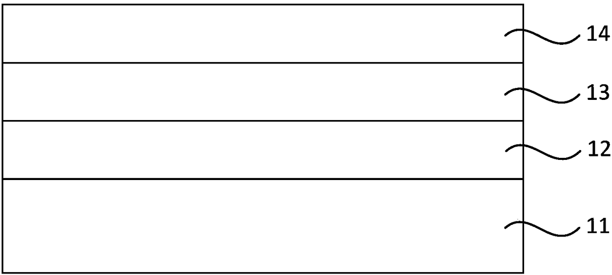
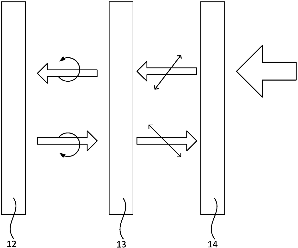
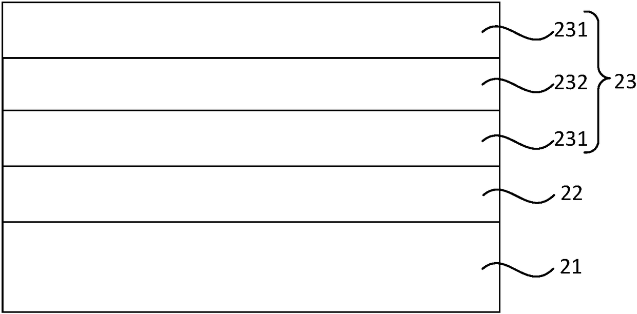
[0033] Figure 2a It is a schematic structural diagram of a display panel according to the second embodiment of the present invention, Figure 2b for Figure 2a Provided a working schematic of the display panel. The technical solution of this embodiment is a specific example of the display panel provided in Embodiment 1, and N is equal to 1 in this embodiment.

[0034] see Figure 2a , the display panel includes a substrate 21, an organic light-emitting device 22 arranged on the substrate 21, and an anti-reflection film 23 arranged on the organic light-emitting device 22. The anti-reflection film 23 includes two first film layers 231 and one second film layer 232 that are stacked. The second film layer 232 is located between two adjacent first film layers 231 , and the two first film layers 231 and the one second film layer 232 together form a sandwich structure. The refractive index of the first film layer 231 is greater than the refractive index of the second film layer...

Embodiment 3

[0042] image 3 This is a schematic structural diagram of a display panel according to Embodiment 3 of the present invention. Compared with the above embodiments, the display panel provided in this embodiment further includes a thin film encapsulation layer covering the organic light emitting device, and the anti-reflection film is disposed on the side of the thin film encapsulation layer away from the organic light emitting device.

[0043] see image 3 , the display panel includes a substrate 21 . The substrate 21 is divided into a plurality of pixel regions 31 and non-pixel regions 32 , and the pixel regions 31 and the non-pixel regions 32 are arranged at intervals. The non-pixel region 32 includes the thin film transistor 24 formed on the substrate 21 , and the pixel defining layer 25 formed on the side of the thin film transistor 24 away from the substrate 21 . The organic light emitting device 22 is included in the pixel region 31 . The organic light-emitting device ...


PUM


Abstract

The embodiment of the invention discloses a display panel and a display device. The display panel comprises a substrate, an organic light-emitting device arranged on the substrate and an anti-reflection film arranged on the organic light-emitting device, wherein the anti-reflection film comprises N+1 first films and N second films alternately stacked and arranged, and N is a positive integer of greater than or equal to 1, wherein the refractive index of the first films is greater than that of the second films. Through the technical scheme, the problems that the bending resistance of the display panel is relatively low and the display brightness of the display panel is reduced caused by the fact that an existing display panel comprises a polaroid are solved, and the purposes of improving the bending resistance and the display brightness of the display panel are achieved under the premise of guaranteeing relatively low reflectivity of the display panel for external light.

Description

technical field [0001] Embodiments of the present invention relate to display technologies, and in particular, to a display panel and a display device. Background technique [0002] Organic light Emitting Display (OLED) has become one of the key directions of the development of the display industry due to its technical advantages such as no need for a backlight, high contrast, thin thickness, wide viewing angle, fast response, and good bending resistance. [0003] In order to improve the contrast ratio and outdoor readability of the display panel, a polarizer is usually provided on the current display panel to reduce the reflectivity of the display panel to external light. Figure 1a It is a schematic structural diagram of an existing display panel. Figure 1b for Figure 1a Schematic diagram of the working principle of the display panel. see Figure 1a and Figure 1b , the display panel includes a substrate 11 , an organic light-emitting device 12 , a quarter-wave plate 1...

Claims


Application Information

Patent Timeline
Patent Type & Authority Applications(China)
IPC IPC(8): H01L51/52H01L27/32
CPCH10K59/00H10K50/84H10K50/86
Inventor 王历平
Owner EVERDISPLAY OPTRONICS (SHANGHAI) CO LTD
Why Eureka
Try Eureka