Manufacturing method of LED array device

A technology of LED array and manufacturing method, which is applied in the direction of identification devices, instruments, electrical components, etc., and can solve the problems of slow transfer speed, low efficiency, and difficulty in mass production of micro-LED displays

Active Publication Date: 2018-10-19
SHANTOU GOWORLD DISPLAY TECH CO LTD
View PDF9 Cites 60 Cited by
  • Summary
  • Abstract
  • Description
  • Claims
  • Application Information

AI Technical Summary

Problems solved by technology

In the prior art, a large amount of tiny LED devices are transferred and bonded to the base layer of the driving circuit to form an LED array device as the main body of the micro LED display, and a transfer head i

Method used


Image

  • Manufacturing method of LED array device
  • Manufacturing method of LED array device
  • Manufacturing method of LED array device

Examples


Embodiment 1

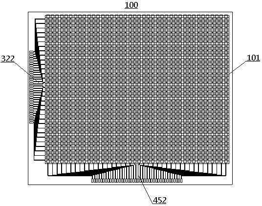
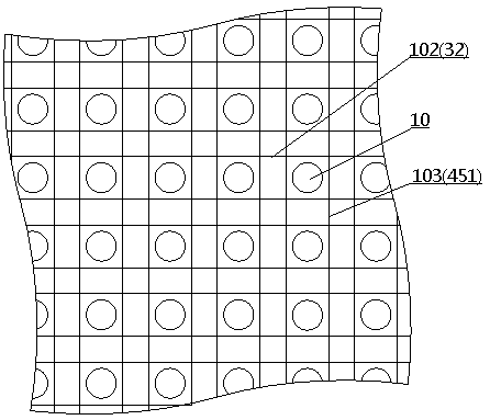
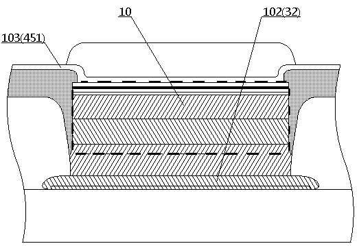
[0098] Embodiment 1 provides the manufacturing method of LED display 100, such as figure 1 , 2 As shown, display 100 is a passively driven monochrome LED display having a pixel area of ​​1.61 inches and a resolution of 40×32. The main body of the display 100 is an LED array 101, which includes 40×32 LED devices 10 arranged in a square matrix, and the pitch of the LED devices 10 is 0.8mm. The LED array 101 is driven by intersecting row electrodes 102 and column electrodes 103, and each pixel has image 3 The cross-sectional structure shown.

[0099] Such as Figure 4 As shown, the LED device 10 is a GaN-based blue light vertical circular LED device with a standard diameter of 0.3mm, and its film layers are the first bonding layer 11, the soft magnetic metal layer (the first magnetic part) from the inside to the outside. ) 12, non-magnetic metal layer 13, first electrode 14 and semiconductor layer 15. Among them, the first bonding layer 11 is a 5 μm thick tin metal layer, t...

Embodiment 2

[0123] Such as Figure 32 As shown in —34, what the second embodiment will make is an active matrix driven color LED display 200, which has a pixel area of ​​26 inches and a resolution of 1920×1080, and each pixel 201 further includes a red (R) , green (G), blue (B), and white (W) sub-pixels 202 in four primary colors. The main body of the display 200 is an LED array 203, which includes a total of 8,294,400 LED devices 10 arranged in a square matrix of 1920×1080×4, and the pitch of the LED devices 10 is 150 μm.

[0124] The LED device 10 of the second embodiment is basically the same as that of the first embodiment (refer to Figure 4 ), the difference is that the diameter of the LED device in Embodiment 2 is 100 μm, the thickness of the soft magnetic metal layer and the copper metal layer are both 20 μm, and the first bonding layer is changed to an indium metal layer with a thickness of 3 μm. The LED device is suspended in DI water to form a dispersion liquid with a dispers...

Embodiment 3

[0135] Such as Figure 54 As shown, the display 300 to be produced in the third embodiment is basically the same as that in the second embodiment, the difference is that each pixel 301 includes a red sub-pixel (R sub-pixel) 3021, a blue sub-pixel 3022 (B sub-pixel ) and two green sub-pixels 3023 (G sub-pixels). In order to save the setting step of the colored layer, the third embodiment uses LED devices of three colors, which are red LED 101 (GaAs LED), blue LED 102 (GaN LED) and green LED 103 (GaP LED). The diameters of the LED devices are 100 μm, 162 μm and 50 μm respectively, and their structures and manufacturing steps (epitaxy substrates used and process parameters may be different) are the same as those of the LED devices used in Example 2, and they are made into DI aqueous dispersions 1911, 1911, and 1911 respectively. 1912 and 1913.

[0136] The design and fabrication steps of the motherboard, base layer and driving circuit layer of the third embodiment are basically...


PUM

PropertyMeasurementUnit
Thicknessaaaaaaaaaa
Melting pointaaaaaaaaaa
Thicknessaaaaaaaaaa

Abstract

A manufacturing method of an LED array device uses LED devices with a vertical structure and a mother board, wherein the LED device is provided with a first magnetic part composed of soft magnetic metal; the mother board is provided with a second magnetic part composed of a hard magnetic material, and a base layer without magnetic insulation is arranged on a first plate surface; a driving circuitlayer including a plurality of welding pads arranged on the base layer, and the welding pads are corresponding to the second magnetic part; the LED devices are distributed on the driving circuit layer, the first magnetic part of the LED device is subjected to the acting force of the magnetic field of the welding pad on the second magnetic part, so that the LED device is arranged on the welding padin a positioning way; so that the LED device and the welding pad are bonded with each other; the base layer and the mother board are separated from each other to obtain an LED array device. This approach can quickly and efficiently transfer large amounts of LED devices to the driving circuit layer.

Description

technical field [0001] The invention relates to a method for manufacturing an LED array device, and belongs to the technical field of LED displays, especially micro LED displays. Background technique [0002] Micro-LED displays such as micro-LEDs or mini-LEDs are generally displays formed by transferring and bonding a large number of tiny light-emitting diodes (LEDs) to a base layer of a driving circuit. Micro-LED displays have the advantages of good display performance (active luminescence, high brightness, high contrast, high color gamut, wide viewing angle, fast response), energy saving, and long working life, and are considered to be more advanced displays than liquid crystal displays and organic light-emitting displays. Types of. In the prior art, a large amount of tiny LED devices are transferred and bonded to the base layer of the driving circuit to form an LED array device as the main body of the micro LED display, and a transfer head is generally used to transfer o...

Claims


Application Information

Patent Timeline
IPC IPC(8): G09F9/33
CPCG09F9/33H01L33/005H01L33/0062H01L33/0075H01L33/32H01L33/36H01L33/44
Inventor 沈奕吕岳敏
Owner SHANTOU GOWORLD DISPLAY TECH CO LTD
Why Eureka
Try Eureka