Method for optimizing the impedance continuity of PCB high-speed link

A high-speed link and continuity technology, applied in the server field, can solve problems such as reducing the integrity of the reference plane, affecting the quality of signal transmission, and affecting the distribution of current flow, so as to optimize the placement of capacitors, improve the quality of signal transmission, and optimize impedance. The effect of continuity

CN108684137AInactive Publication Date: 2018-10-19ZHENGZHOU YUNHAI INFORMATION TECH CO LTD
5 Cites 4 Cited by

Patent Information

Authority / Receiving Office
CN · China
Current Assignee / Owner
Publication Date
2018-10-19
Estimated Expiration
Not applicable · inactive patent

Smart Images

  • Figure 1
    Figure 1
  • Figure 2
    Figure 2
  • Figure 3
    Figure 3
Patent Text Reader

Abstract

The invention discloses a method for optimizing the impedance continuity of a PCB high-speed link. The PCB high-speed link comprises a main board and a receiving card, which are connected through a connector. The main board comprises a transmitting end and a capacitor, and the receiving card comprises a receiving end. The method comprises the following steps of adjusting the position of the capacitor, and performing time-domain reflectometer simulation according to different positions of the capacitor; comparing the high-speed link impedance and loss feature of the PCB under different positions of the specific capacitance; according to the comparing result, the optimal position of the capacitor can be determined. The invention is advantageous in that the time domain reflectometer result ofthe simulation link is conducted through changing the capacitance placement position, the capacitance placement position is optimized, so that the overall impedance continuity of the link is best, and the signal transmission quality is improved.
Need to check novelty before this filing date? Find Prior Art

Description

technical field

[0001] The invention relates to the technical field of servers, in particular to a method for optimizing the continuity of PCB high-speed link impedance. Background technique

[0002] In traditional digital system design, high-speed interconnect phenomena are often negligible because they have little impact on system performance. However, with the continuous development of computer technology, high-speed interconnection is playing a leading role among many factors that determine system performance, which often leads to some unforeseen problems and greatly increases the complexity of system design. Therefore, in the design of high-speed links, it is necessary to optimize each module as much as possible, evaluate the design feasibility and risk points in advance with the help of simulation tools, and optimize the design based on the simulation results to improve the success rate of system design and shorten the development cycle.

[0003] In the design process...

Examples

Embodiment Construction

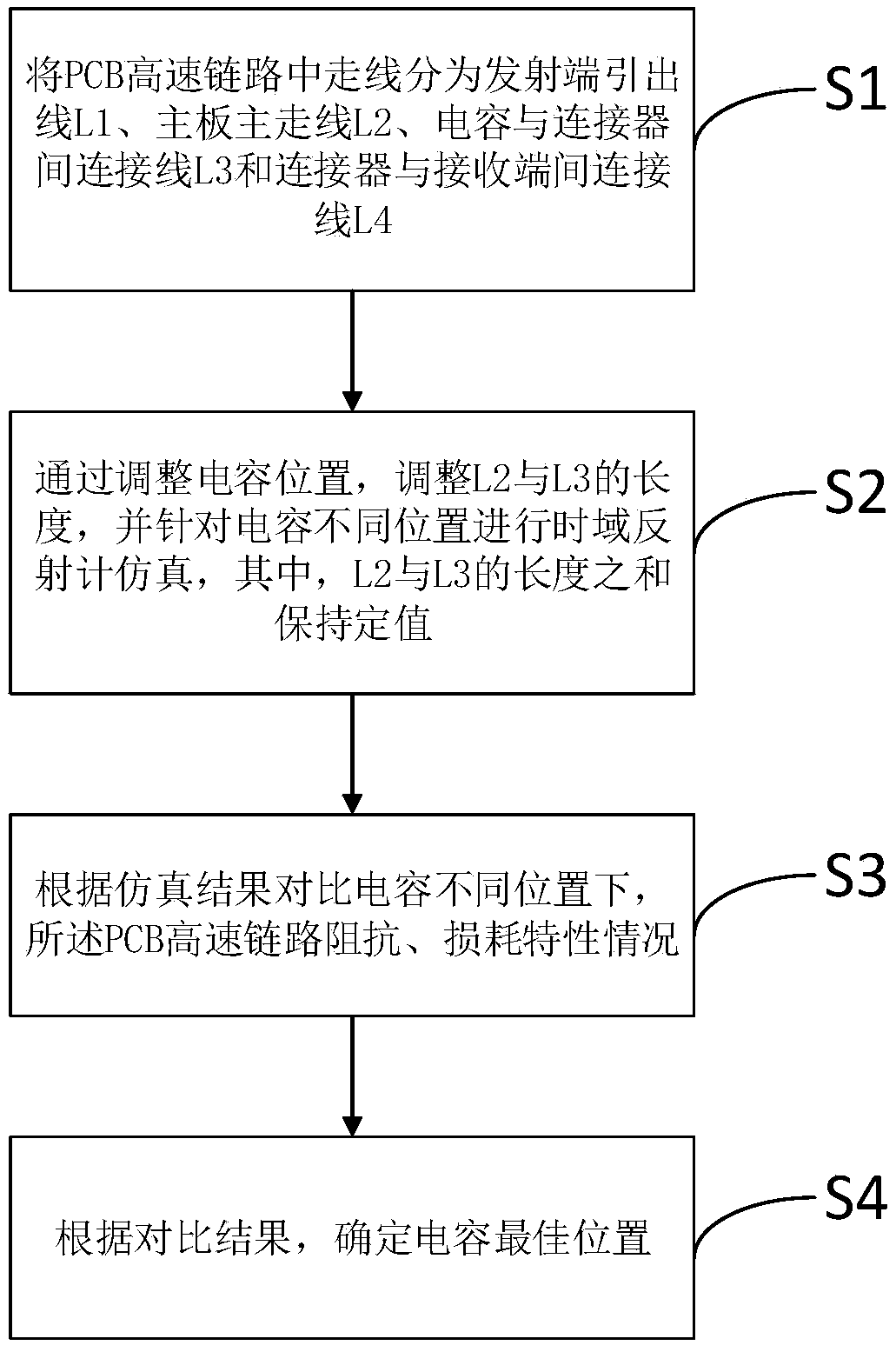
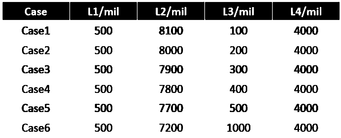
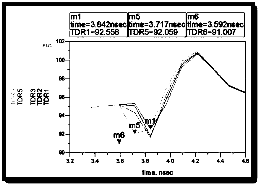
[0021] Such as Figure 1-5 as shown, figure 1 A flow chart of a method for optimizing PCB high-speed link impedance continuity proposed by the present invention; figure 2 It is a diagram of simulation items for different placement positions of capacitors; image 3 It is the simulation diagram of the link time domain reflectometer at different positions of the capacitor; Figure 4 It is the simulation diagram of the link insertion loss at different positions of the capacitor; Figure 5 It is the simulation diagram of the return loss of the link at different positions of the capacitor.

[0022] The present invention will be described in detail below in conjunction with the accompanying drawings and embodiments.

[0023] A method for optimizing PCB high-speed link impedance continuity, comprising the following steps:

[0024] S1: Divide the wiring in the PCB high-speed link into the lead-out line L1 of the transmitter, the main wiring L2 of the main board, the connecting li...