An organic electroluminescent device

An electroluminescent device and a luminescent technology, applied in the direction of electric solid-state devices, electrical components, semiconductor devices, etc., can solve the problems of fast device efficiency roll-off, short luminous life, etc., and achieve reduced efficiency roll-off phenomenon and high luminous efficiency , the effect of improving efficiency

Active Publication Date: 2019-07-16
KUNSHAN GO VISIONOX OPTO ELECTRONICS CO LTD +1
View PDF6 Cites 0 Cited by
  • Summary
  • Abstract
  • Description
  • Claims
  • Application Information

AI Technical Summary

Problems solved by technology

[0006] Therefore, the technical problem to be solved by the present invention is to overcome the triplet-triplet annihilation (TTA), triplet-polaron Annihilation (TPA) and singlet-triplet annihilation (STA) phenomena are serious, resulting in the defects of fast roll-off of device efficiency and short luminous lifetime

Method used


Image

  • An organic electroluminescent device
  • An organic electroluminescent device
  • An organic electroluminescent device

Examples


Embodiment 1

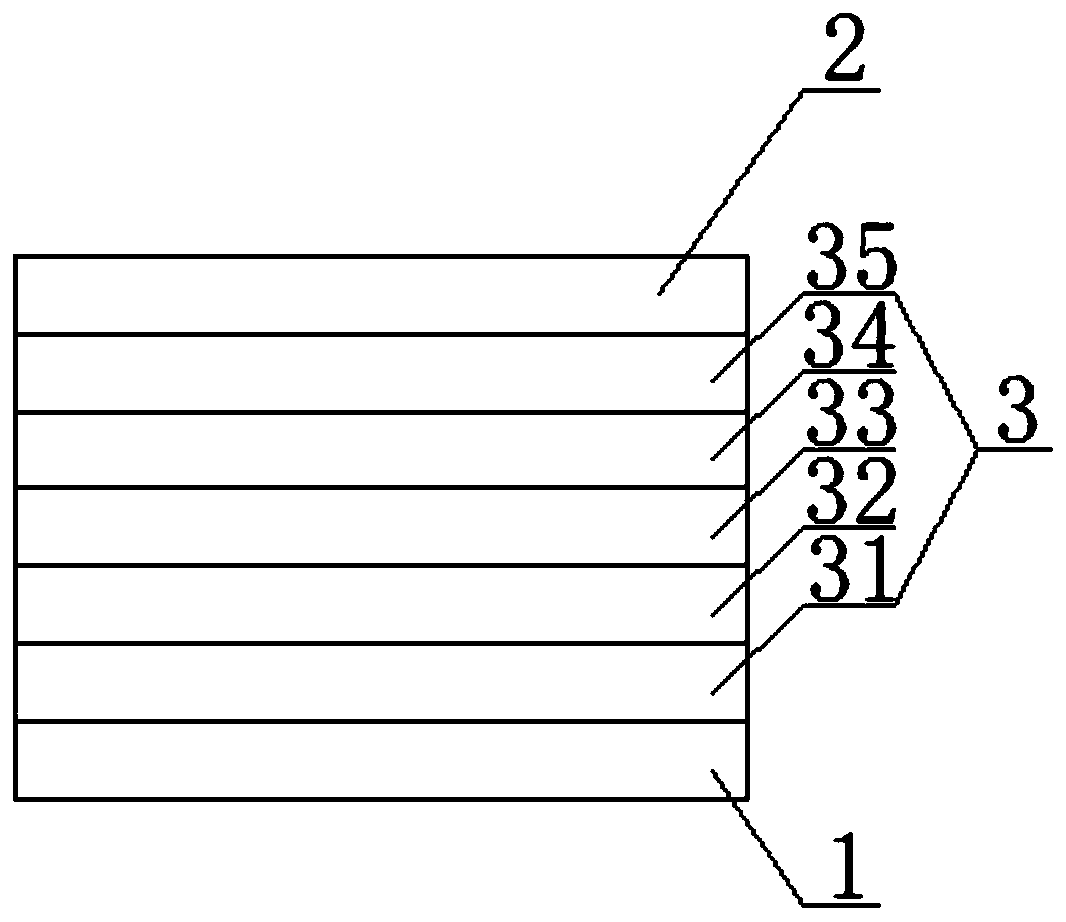
[0063] This embodiment provides an organic electroluminescent device, such as figure 2 As shown, it includes a first electrode 1, a second electrode 2, and an organic functional layer 3 located between the first electrode 1 and the second electrode. Among them, the first electrode 1 is an anode, the second electrode 2 is a cathode, and the organic functional layer 3 includes a hole injection layer 31, a hole transport layer 32, a light emitting layer 33, an electron transport layer 34 and Electron injection layer 35.

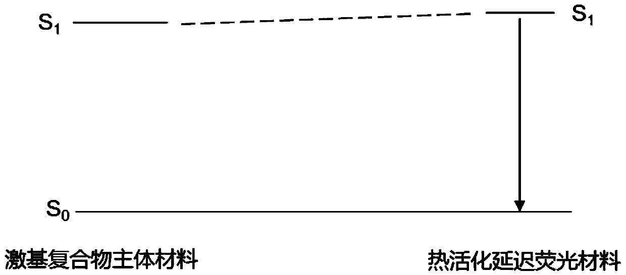
[0064] The light-emitting layer 33 is composed of a host material doped with a guest material. The host material is an exciplex with electron transport properties and hole transport properties, and the guest material is a thermally activated delayed fluorescent material. The doping ratio of the thermally activated delayed fluorescent material is (The ratio of the mass of the thermally activated delayed fluorescent material to the total mass of the light-emitting l...

Embodiment 2

[0080] This embodiment provides an organic electroluminescence device. The structure of the organic electroluminescence device is the same as that of embodiment 1. The difference between the organic electroluminescence device and the organic electroluminescence device provided in embodiment 1 is only: the formation of exciplex The mass ratio of the electron donor material (D-20) and the electron acceptor material (A-30) is 7:3. The organic electroluminescent device has the following device structure:

[0081] ITO / HATCN(5nm) / NPB(30nm) / TCTA(10nm) / 63wt%(D-20): 27wt%(A-30): 10wt%(T-3)(30nm) / 50wt% DpyPA: 50wt% Liq(30nm) / LiF(0.5nm) / Al(150nm).

[0082] The singlet energy level of the exciplex is 2.86 eV, and the singlet energy level of the thermally activated delayed fluorescent material (T-3) is 2.90 eV.

Embodiment 3

[0084] This embodiment provides an organic electroluminescence device. The structure of the organic electroluminescence device is the same as that of embodiment 1. The difference between the organic electroluminescence device and the organic electroluminescence device provided in embodiment 1 is only: the main body of the light-emitting layer 33 The material is electron donor material (D-20) and electron acceptor material (A-19) to form exciplex, the mass ratio of electron donor material (D-20) and electron acceptor material (A-19) is 1:1; the doping ratio of the thermally activated delayed fluorescent material (T-3) as the guest material in the light-emitting layer 33 is 20 wt%. The organic electroluminescent device has the following device structure:

[0085] ITO / HATCN(5nm) / NPB(30nm) / TCTA(10nm) / 40wt%(D-20):40wt%(A-19):20wt%(T-3)(30nm) / 50wt%DpyPA:50wt% Liq(,30nm) / LiF(0.5nm) / Al(150nm).

[0086] The singlet energy level of the exciplex is 2.86 eV, and the singlet energy level of t...


PUM


Abstract

The invention discloses an organic electroluminescent device. The luminescent layer includes a host material and a guest material. The host material is an exciplex formed by an electron donor material and an electron acceptor material, and the guest material is a thermally activated delayed fluorescent material. , the singlet energy level of the host material is lower than that of the guest material. Since the singlet energy level of the exciplex as the host material in the light-emitting layer is lower than that of the thermally activated delayed fluorescent material, the generation of high-energy excitons is avoided, and the molecular bond breakage caused by high excitation energy is effectively suppressed; The singlet energy level of the exciplex is low, which is beneficial to reduce the excitation energy of the excitons in the device, and suppress the triplet-triplet annihilation, triplet-polaron annihilation and singlet-triplet annihilation in the device. Reduce the efficiency roll-off of the device and prolong the life of the device.

Description

Technical field [0001] The invention belongs to the field of display technology, and specifically relates to an organic electroluminescence device. Background technique [0002] Organic light-emitting diodes (OLED) have great application prospects in the display and lighting fields due to their advantages such as ultra-thin, light weight, low energy consumption, active light emission, wide viewing angle, and fast response. People pay more attention. [0003] In 1987, C.W.Tang and Vanslyke of Eastman Kodak in the United States reported for the first time a double-layer organic electroluminescent device based on Alq3 and triarylamines, which opened the direction of OLED research. Traditional fluorescent materials are easy to synthesize, inexpensive, stable, and have a long device life. However, due to electron spin forbidden, only 25% of singlet excitons can be used to emit light, and the external quantum efficiency of the device is often less than 5%. Need to be further improved. ...

Claims


Application Information

Patent Timeline
Patent Type & Authority Patents(China)
IPC IPC(8): H01L51/50H01L51/54
CPCH10K85/624H10K85/654H10K50/12
Inventor 段炼李熠烺宋晓增张东东李国孟
Owner KUNSHAN GO VISIONOX OPTO ELECTRONICS CO LTD
Why Eureka
Try Eureka