

Wideband bidirectional wide-angle absorbing structure and preparation method thereof
A wave structure and wide-angle technology, applied in the field of broadband bidirectional wide-angle wave absorbing structure and its preparation, can solve problems such as working band limitation, and achieve the effects of low preparation cost, simple design, convenient and rapid mass production
- Summary
- Abstract
- Description
- Claims
- Application Information
AI Technical Summary
Problems solved by technology
Method used
Image

Examples
Embodiment 1
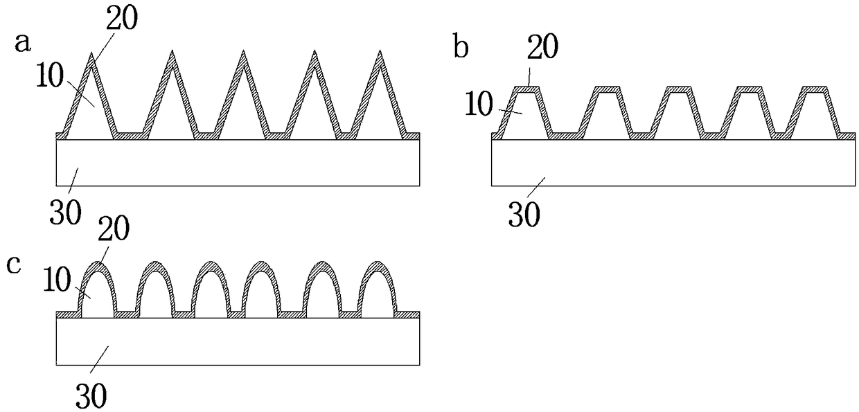
[0043] see figure 1 , the ultra-broadband bidirectional wide-angle wave absorbing structure of the present invention comprises a moth-eye nanostructure array, and the moth-eye nanostructure array is formed on the upper surface of the substrate 30, and the material of the substrate 30 is PET, PMMA, quartz, UV resin, polycarbonate or GaAs .
[0044] The upper surface of the moth-eye nanostructure array junction is covered with a metal layer 20, and the material of the metal layer 20 can be selected from metals such as nickel, chromium, and titanium. The moth-eye nanostructure array is composed of several quasi-periodic moth-eye nanostructures 10. In the horizontal direction, the width of the end of the moth-eye nanostructure 10 close to the metal layer 20 is smaller than the width of the end away from the metal layer 20 (that is, the width at the bottom and the width at the top). ratio greater than 1:1), see figure 1 , moth-eye nanostructures have various shapes, such as nanos...
Embodiment 2
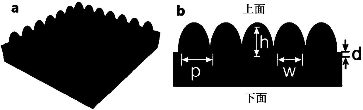
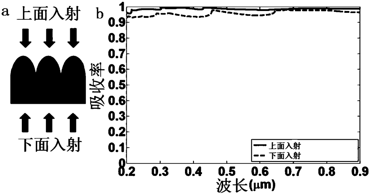
[0047] The ultra-broadband bidirectional wide-angle wave-absorbing structure of the present invention has a high wave-absorbing rate for ultraviolet to near-infrared wavebands. In a preferred embodiment of the present invention, the metal layer of the wave absorbing structure adopts metal nickel. The period p of the moth-eye nanostructure array is 350 nm, the duty cycle F is 0.8, the height h of the moth-eye nanostructure array is 1000 nm, and the thickness of the metal layer is 40-100 nm. image 3 is when light is incident from above and below ( image 3 a), the graph of the relationship between the absorbing efficiency and the wavelength of the ultra-broadband bidirectional wide-angle absorbing structure of the present invention ( image 3 b). like image 3 As shown, in the ultraviolet to near-infrared band, the ultra-broadband bidirectional wide-angle wave absorbing structure of the present invention has a wave absorption rate of over 98%, and at specific wavelengths (eg...
Embodiment 3
[0051] In this embodiment, the structural parameters of the ultra-broadband bidirectional wide-angle absorbing structure are: the period p is 250-550 nm, the thickness d of the metal layer is 80 nm, and the ratio (h / p) of the height to the period of the moth-eye nanostructure array is 3, The ratio of the width w of the bottom of the moth-eye nanostructure to the period p is F=0.7.
[0052] Figure 5 a-5b is a graph of the relationship between the period p and the absorption rate of the ultra-broadband bidirectional wide-angle wave absorbing structure of the present invention when light is incident from above and below (the unit of period p in the figure is microns). It can be seen that when incident from above, the period varies in the range of 250-500nm, and the structure obtains high absorption efficiency (>90%) in the wavelength range of 200-3000nm; the period varies in the range of 250-450nm, and the structure is in the range of 1000-1750nm waveband, the absorbing efficie...
PUM
 Abstract
Description
Claims
Application Information