
Device for manufacturing large-are micro-nanostructures in batches and working method of device

A micro-nano structure, large-area technology, applied in the direction of nanotechnology, pattern surface photolithography, instruments, etc., can solve the problem of uneven exposure, meet the requirements of high precision, ensure consistency, and simplify equipment structure and the effect of the steps

Pending Publication Date: 2018-11-06
QINGDAO TECHNOLOGICAL UNIVERSITY
View PDF3 Cites 3 Cited by
  • Summary
  • Abstract
  • Description
  • Claims
  • Application Information

AI Technical Summary

Problems solved by technology

(3) The UV LED lamp line / surface light source is used as the light source for curing the imprinting material. Since the line / surface light source is irradiated vertically on the workbench, as the workbench moves, the UV LED lamp will be irradiated on the imprint material in turn. Complete curing, which solves the problem of uneven exposure, can obtain high-quality embossed graphics, and simplifies the equipment structure and operation steps

Method used

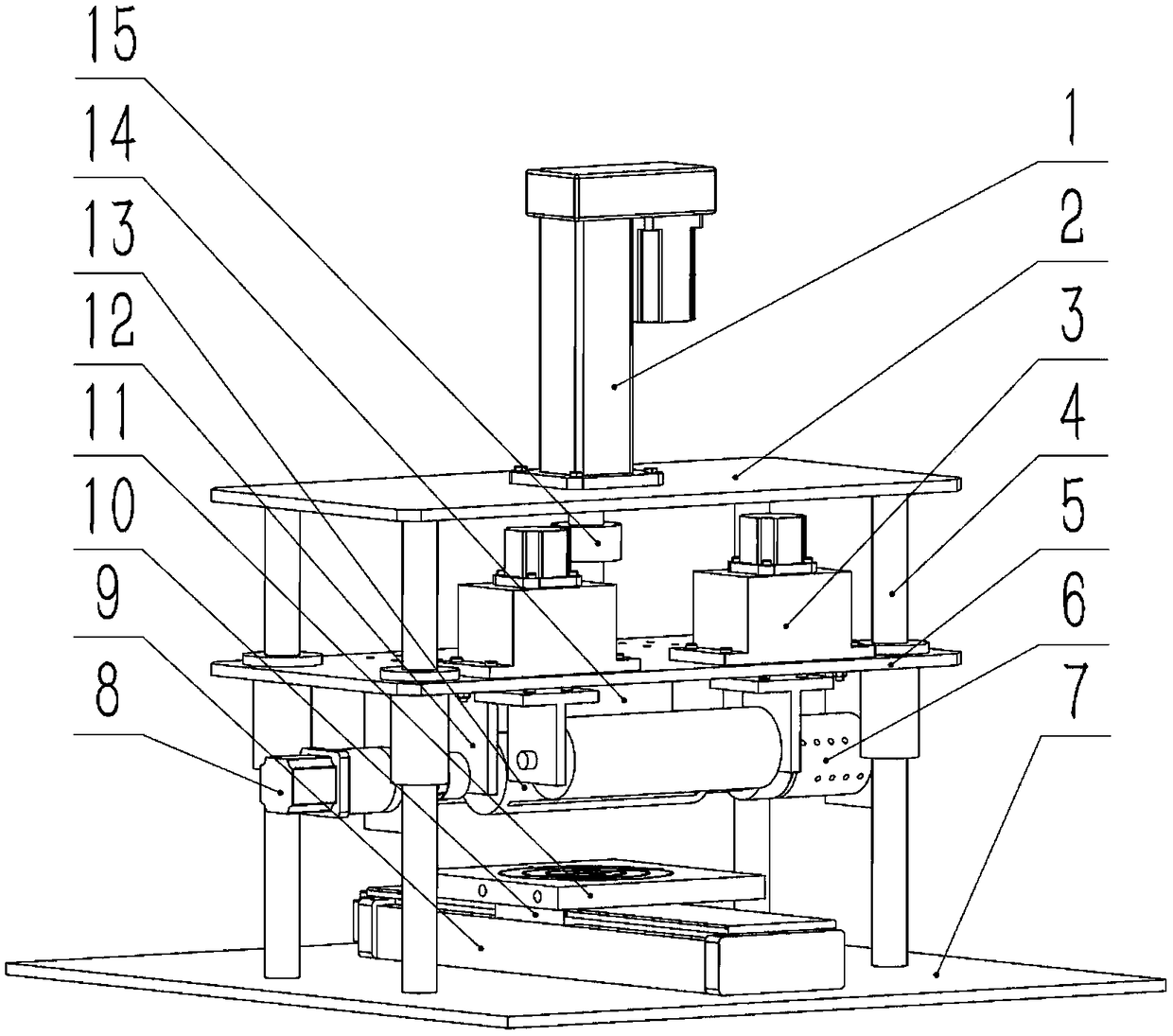
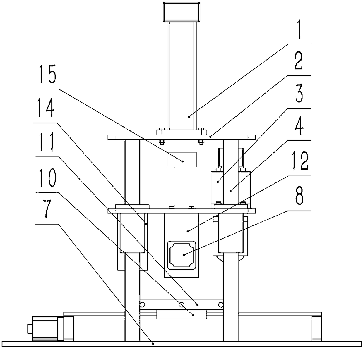
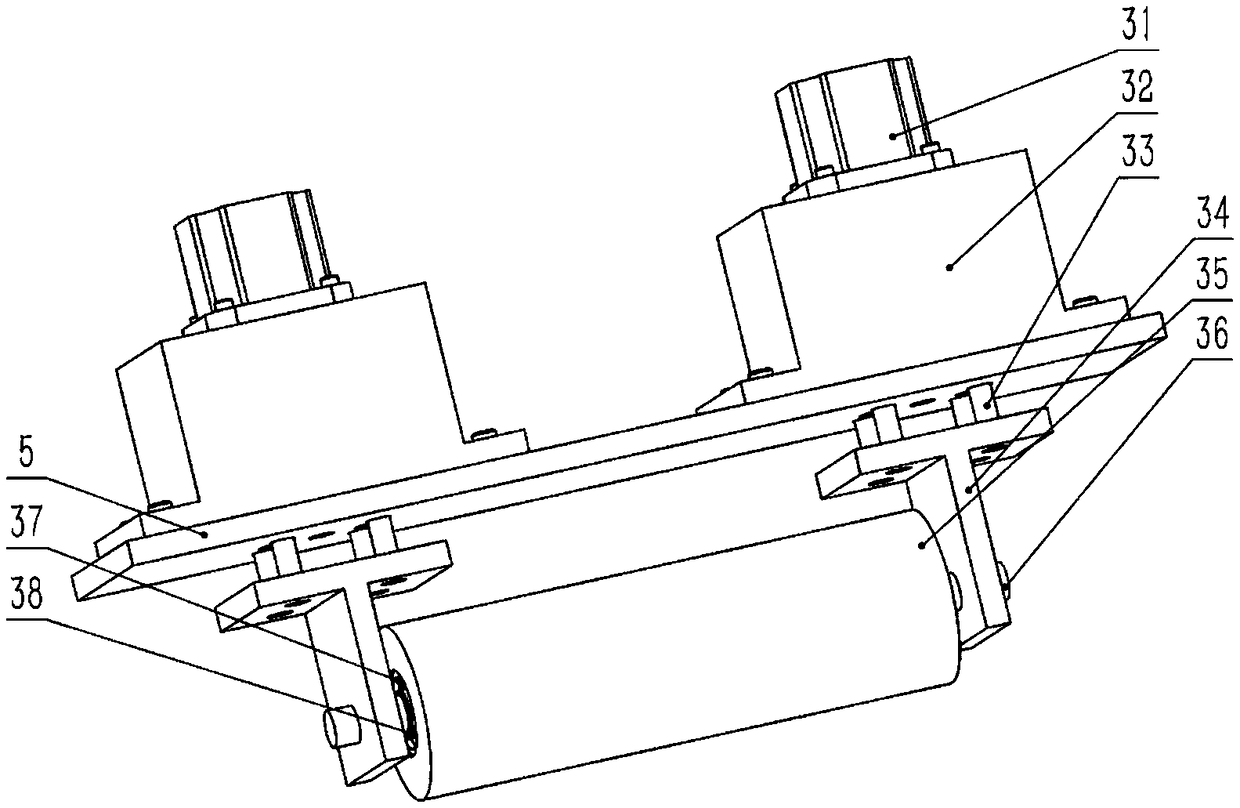

Image

  • Device for manufacturing large-are micro-nanostructures in batches and working method of device
  • Device for manufacturing large-are micro-nanostructures in batches and working method of device
  • Device for manufacturing large-are micro-nanostructures in batches and working method of device

Examples


Embodiment Construction

[0067] It should be pointed out that the following detailed description is exemplary and intended to provide further explanation to the present application. Unless defined otherwise, all technical and scientific terms used herein have the same meaning as commonly understood by one of ordinary skill in the art to which this application belongs.

[0068] It should be noted that the terminology used here is only for describing specific implementations, and is not intended to limit the exemplary implementations according to the present application. As used herein, unless the context clearly dictates otherwise, the singular is intended to include the plural, and it should also be understood that when the terms "comprising" and / or "comprising" are used in this specification, they mean There are features, steps, operations, means, components and / or combinations thereof.

[0069] As introduced in the background technology, there are deficiencies in the prior art. In order to solve th...


PUM

PropertyMeasurementUnit
thicknessaaaaaaaaaa
diameteraaaaaaaaaa
heightaaaaaaaaaa

Abstract

The invention discloses a device for manufacturing large-are micro-nanostructures in batches and a working method of the device. According to the device, the precision and the quality of imprinted patterns and the efficiency and the reliability of micro-nano imprinting equipment are improved, and the service life of a mold is prolonged. According to the technical scheme, the device comprises a base plate, vertical guide rods are fixedly arranged on the base plate, the tops of the guide rods are fixedly connected with a top plate, a support plate is arranged in the middles of the guide rods ina penetrating mode, a driving device is connected with the support plate to drive the support plate to move up and down, and a pressure detection module is arranged between the driving device and thesupport plate; and an auxiliary imprinting module, a main imprinting module and a solidification module are sequentially connected to the bottom of the support plate from front to back, the auxiliaryimprinting module comprises an imprinting roller, a roller shaft is arranged in the middle of the imprinting roller in a penetrating mode, the two ends of the roller shaft are connected with imprinting roller connecting frames, the tops of the imprinting roller connecting frames are connected with a reciprocating mechanism through auxiliary imprinting module guide rods, and the reciprocating mechanism can drive the imprinting roller to move up and down.

Description

technical field [0001] The invention relates to the technical field of micro-nano manufacturing, in particular to a device for mass-manufacturing large-area micro-nano structures and a working method thereof. Background technique [0002] In order to improve and improve the performance and quality of products in the fields of high-definition flat panel display, high-efficiency solar panels, anti-reflection and self-cleaning glass, LED patterning, OLED, LCD, and wafer-level micro-nano optical devices, for large-area micro-nano structure batches There is a huge industrial demand for chemical manufacturing technology. The common feature of these products is that large-area complex three-dimensional micro-nano structures need to be manufactured efficiently and at low cost on large-scale non-flat rigid substrates (hard substrates or substrates). However, various existing micro-nano manufacturing technologies (such as electron beam lithography, optical lithography, laser interfer...

Claims


Application Information

Patent Timeline
Patent Type & Authority Applications(China)
IPC IPC(8): G03F7/00B82Y40/00
CPCG03F7/0002B82Y40/00
Inventor 兰红波刘明杨许权
Owner QINGDAO TECHNOLOGICAL UNIVERSITY
Learn More