Gate driver monolithic and repairing method thereof
A gate drive circuit and path technology, applied in the direction of instruments, static indicators, etc., can solve problems such as unfavorable repair, complex repair, and inability to achieve thin-film transistor-level repair, etc., and achieves a reduction in the probability of damage or damage and a reduction in area. Effect
- Summary
- Abstract
- Description
- Claims
- Application Information
AI Technical Summary
Problems solved by technology
Method used
Image
Examples
Embodiment 1
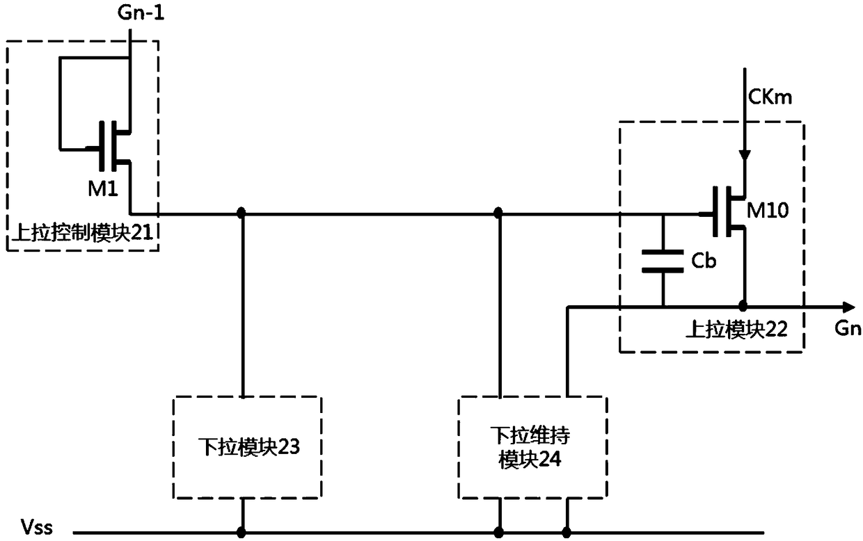
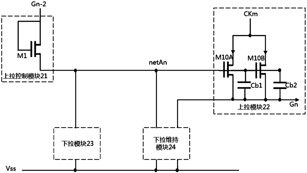
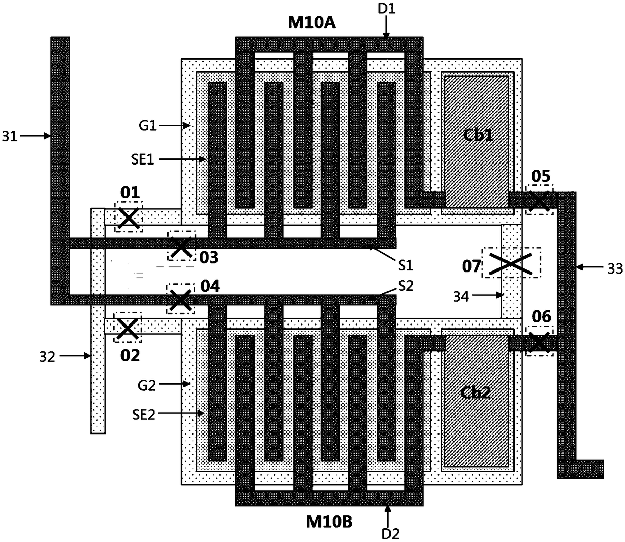
[0060] Such as figure 2 As shown, the first original thin film transistor M10 in the pull-up module 22 (such as figure 1 ) is replaced by the first thin film transistor M10A and the second thin film transistor M10B, and spaces for laser cutting of the gate, source and drain of the first thin film transistor M10A and the second thin film transistor M10B are reserved on the layout.
[0061] The first thin film transistor M10A and the second thin film transistor M10B are smaller in area and channel width than the first original thin film transistor M10 .
[0062] Specifically, the pull-up module 22 includes a clock signal input terminal 31, a first pull-up control node terminal 32, a gate scanning signal output terminal 33, a double-gate connection terminal 34, a first thin film transistor M10A, a second thin film transistor M10B, a first A capacitor Cb1 and a second capacitor Cb2; the clock signal input terminal 31 inputs the first clock signal CKm, the first pull-up control n...
Embodiment 2
[0075] Such as Figure 4 As shown, the second original thin film transistor M1 in the pull-up control module 21 (such as figure 1 ) is replaced by the third thin film transistor M1A and the fourth thin film transistor M1B, and spaces for the third thin film transistor M1A and the fourth thin film transistor M1B to realize laser cutting of the gate, source and drain are reserved on the layout.
[0076] The first thin film transistor M1A and the second thin film transistor M1B are smaller in area and channel width than the second original thin film transistor M1.
[0077] Specifically, as Figure 5 As shown, the pull-up control module 21 includes a pull-up control signal input terminal 41, a second pull-up control node terminal 42, a first metal line connection terminal 43, a second metal line connection terminal 44, a third thin film transistor M1A and a fourth For the thin film transistor M1B, the pull-up control signal input terminal 41 inputs the nth stage pull-up control ...
PUM
 Abstract
Description
Claims
Application Information


