

Preparation method of on-chip high-quality thin film micro-optical structure
A micro-optic, high-quality technology, applied in semiconductor/solid-state device manufacturing, electrical components, circuits, etc., to overcome the difficulties in the coupling region, improve efficiency, and reduce the effective mode volume
- Summary
- Abstract
- Description
- Claims
- Application Information
AI Technical Summary
Problems solved by technology
Method used
Image

Examples
Embodiment Construction
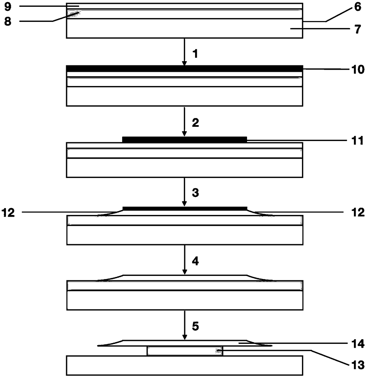
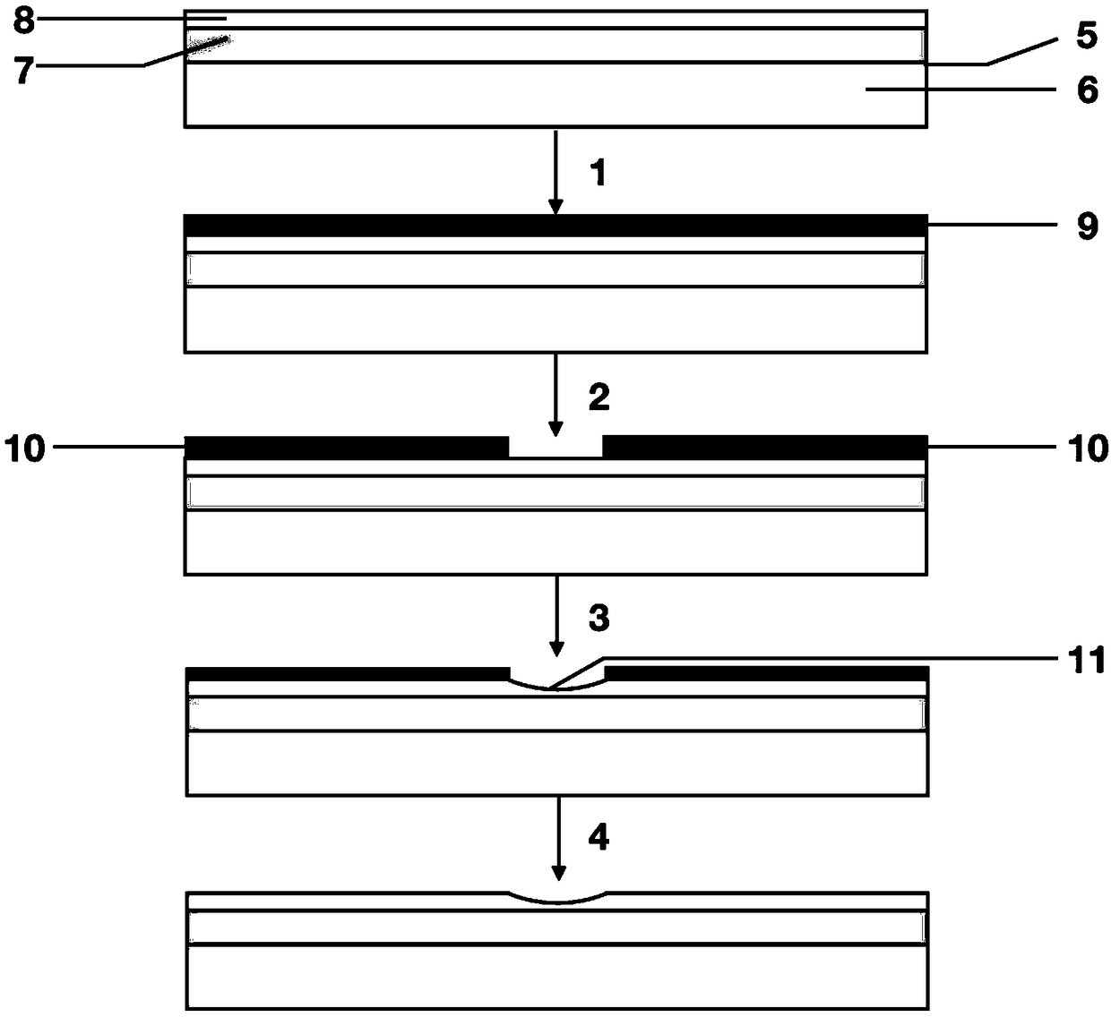
[0030] The present invention will be further described below by examples and accompanying drawings, but the protection scope of the present invention should not be limited by this.
[0031] see first figure 1 , figure 1 It is a schematic flow chart of the method for preparing an on-chip optical whispering gallery mode microcavity by using femtosecond laser combined with chemical mechanical polishing. The method of the present invention is now illustrated by taking the on-chip lithium niobate single crystal thin film as an example. It can be seen from the figure that the present invention uses femtosecond The method for preparing an on-chip optical whispering gallery mode microcavity by combining laser with chemical mechanical polishing includes the following five steps:
[0032] (1) Plating Cr metal film on the surface: Take an on-chip single crystal lithium niobate film sample 6 with a size of 3mm×4mm×1mm, which consists of a substrate 7 with a thickness of about 1mm, SiO 2...
PUM
| Property | Measurement | Unit |
|---|---|---|
| wavelength | aaaaa | aaaaa |
Abstract
Description
Claims
Application Information