Air tightness surface acoustic wave element package structure and manufacturing method thereof

A surface acoustic wave, packaging structure technology, applied in electrical components, impedance networks, etc., can solve problems such as large differences in expansion coefficients, limiting process throughput, and difficulty in cutting piezoelectric wafers

Inactive Publication Date: 2018-11-06
张琴
View PDF11 Cites 6 Cited by
  • Summary
  • Abstract
  • Description
  • Claims
  • Application Information

AI Technical Summary

Problems solved by technology

[0008] 2) Cut the piezoelectric material wafer into a single surface acoustic wave element chip (the surface acoustic wave element is very similar to the bare chip of the integrated circuit at this time); due to the hard, brittle and fragile characteristics of the massage material, the piezoelectric wafer Very difficult to cut;
[0011] In this packaging structure, the price of the ceramic substrate used is high; the dimensional stability is poor (using high temperature sintering over 1000 degrees Celsius); in addition, it is difficult to cut. Of

Method used


Image

  • Air tightness surface acoustic wave element package structure and manufacturing method thereof
  • Air tightness surface acoustic wave element package structure and manufacturing method thereof
  • Air tightness surface acoustic wave element package structure and manufacturing method thereof

Examples


Embodiment 1

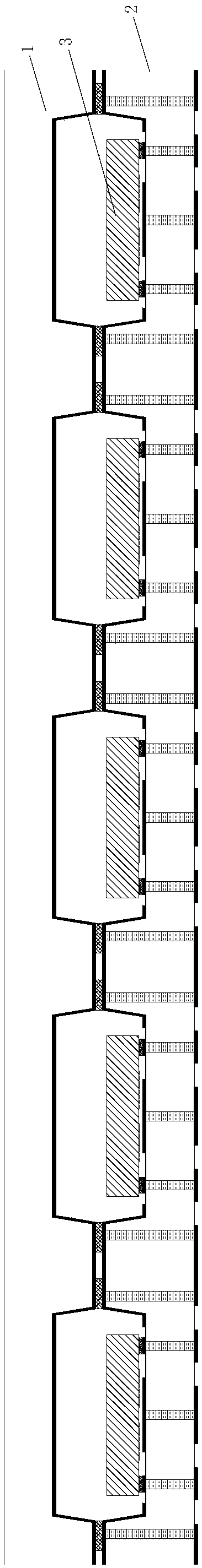
[0156] like Figure 3 ~ Figure 7 As shown, this embodiment provides an airtight surface acoustic wave element packaging structure, which includes an upper glass cover array 1 , a lower glass substrate array 2 and five surface acoustic wave chips 3 .

[0157] The upper glass cover array 1 has five upper glass cover plates 11, each upper glass cover plate 11 corresponds to a surface acoustic wave chip 3, which includes a first glass body 111, and the first glass body 111 etches a first Groove 112, the first groove 112 is facing the corresponding surface acoustic wave chip 3, and the first conductive layer is deposited on the inner surface of the etched first glass body 111, specifically, the first conductive layer is generally made of copper, molybdenum, Made of tungsten, aluminum copper, nickel, etc., the first metal layer 113 is electroplated on the first conductive layer. The first metal layer 113 is made of copper material, which realizes the electromagnetic shielding of the...

Embodiment 2

[0194] The main features of the package structure of the hermetic surface acoustic wave element in this embodiment are as follows: Figure 10 ~ Figure 12 As shown, each upper glass cover 11 of the upper glass cover array includes a first glass body 111, a first conductive layer is deposited on the inner surface of the first glass body 111, and a first metal layer 112 is electroplated on the first conductive layer. , preferably, the surface of the upper glass cover 11 can also be protected with metals such as nickel-palladium-gold, nickel-gold, silver, etc.; furthermore, the upper glass cover 11 can also be printed with an adhesive 113 after metallization. The mixture 113 can align and press the upper glass cover array and the lower glass substrate array; each lower glass substrate 21 includes a second glass body 211, and the second glass body 211 is etched with grooves 212 and through holes 213. The slot 212 is used to mount the corresponding surface acoustic wave chip 3, and ...

Embodiment 3

[0222] The main features of the package structure of the hermetic surface acoustic wave element in this embodiment are as follows: Figure 13 ~ Figure 15 As shown, each upper glass cover 11 of the upper glass cover array includes a first glass body 111, and the first glass body 111 is etched with a groove 112, the groove 112 is facing the corresponding surface acoustic wave chip 3, and the etched The first conductive layer is deposited on the inner surface of the first glass body 111, and the first metal layer 113 is electroplated on the first conductive layer. Preferably, metals such as nickel palladium gold, nickel gold, and silver can also be used on the surface of the upper glass cover plate 11. protection; further, the upper glass cover plate 11 can also be printed with adhesive 114 after metallization, and the upper glass cover plate array and the lower glass substrate array can be aligned and pressed through the adhesive 114; The glass substrate 21 includes a second gla...


PUM

PropertyMeasurementUnit
Thicknessaaaaaaaaaa

Abstract

The invention discloses an air tightness surface acoustic wave element package structure and a manufacturing method thereof. The package structure comprises an upper glass cover plate array, a lower glass substrate array and a plurality of surface acoustic wave chips; a plurality of the surface acoustic wave chips are attached to the lower glass substrate array; the upper glass cover plate array and the lower glass substrate array are aligned and laminated through an adhesive to form a plurality of cavities; a plurality of upper glass cover plates of the upper glass cover plate array, a plurality of lower glass substrates of the lower glass substrate array, a plurality of surface acoustic wave chip and a plurality of the cavities all correspond to one another; and the surface acoustic wavechips are located in the corresponding cavities. The air tightness surface acoustic wave element package structure and the manufacturing method thereof in the invention simplify packaging of the conventional surface acoustic wave component, and greatly increase the throughput of the process, thereby greatly improving the production efficiency.

Description

technical field [0001] The invention relates to a surface acoustic wave component packaging structure, in particular to an airtight surface acoustic wave component packaging structure and a manufacturing method, belonging to the field of surface acoustic wave component packaging. Background technique [0002] Surface Acoustic Wave (SAW, Surface Acoustic Wave) is an elastic wave that propagates along the surface of an object. Surface acoustic wave is a kind of sound wave whose energy is concentrated on the ground surface and propagated by the British physicist Rayleigh (Rayleigh). [0003] In 1965, R.M.White and F.W.Voltmer of the United States published a paper entitled "A New Type of Surface Acoustic Wave Acoustic-Electric Converter", which made metals that can excite surface acoustic waves on the surface of piezoelectric materials. Interdigital Transducer (IDT), realize the mutual conversion of sound waves and electromagnetic waves, see attached Figure 1 . [0004] On t...

Claims


Application Information

Patent Timeline
IPC IPC(8): H03H3/08H03H9/00H03H9/02
CPCH03H3/08H03H9/00H03H9/02535H03H2009/0019
Inventor 张琴
Owner 张琴
Why Eureka
Try Eureka