Absorption structure and manufacturing method thereof

A technology of absorption structure and manufacturing method, which is applied in the field of design and development of photovoltaic technology, can solve problems such as poor absorption effect, and achieve the effect of improving absorption capacity, enhancing absorption effect, and increasing thickness

Inactive Publication Date: 2018-11-13
SHANGHAI JIAO TONG UNIV
View PDF3 Cites 2 Cited by
  • Summary
  • Abstract
  • Description
  • Claims
  • Application Information

AI Technical Summary

Problems solved by technology

[0003] Aiming at the defects in the prior art, the object of the present invention is to propose an absorption layer that solves the problems of poor absorption effect, random structure design,

Method used


Image

  • Absorption structure and manufacturing method thereof
  • Absorption structure and manufacturing method thereof
  • Absorption structure and manufacturing method thereof

Examples


Embodiment Construction

[0034] The present invention will be described in detail below in conjunction with specific embodiments. The following examples will help those skilled in the art to further understand the present invention, but do not limit the present invention in any form. It should be noted that those skilled in the art can make several changes and improvements without departing from the concept of the present invention. These all belong to the protection scope of the present invention.

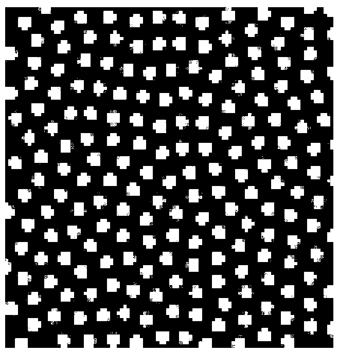
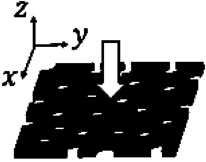
[0035] In the present invention, a hyperuniform absorption structure applicable to thin-film solar cells that is insensitive to the polarization state and incident angle of incident light is composed of an amorphous silicon thin plate 1 with a thickness of 0.2 μm and a subunit size of 4 μm×4 μm. composition. Among them, there are about 140 air holes 2 with a radius of 0.12 μm arranged in the subunit, and the distribution of the air holes 2 follows a super-uniform distribution (short-range order, long-ra...


PUM

PropertyMeasurementUnit
Thicknessaaaaaaaaaa
Radiusaaaaaaaaaa

Abstract

The invention provides an absorption structure and a manufacturing method thereof, wherein the absorption structure is composed of a structural unit and a plurality of through holes arranged on the structural unit and is characterized in that the manufacturing method comprises the following steps: step 1: obtaining a size L of the structural unit; step 2: determining a restricted wave vector rangekc according to the size L; step 3: making the wave vector within the wavenumber range kc satisfy the condition that the structural factor is equal to 0; step 4: obtaining a distribution of the through holes, wherein the distribution of the through holes meets that the value of the structural potential function is the minimum in a molecular dynamics simulation. Compared with the prior art, the absorption structure has the advantages that the absorption structure can be used as a super-homogeneous absorption structure that is not sensitive to polarization state of incident light in a thin filmsolar cell; under a vertical incidence condition, the absorption structure can absorb as much as 67.8% of light in the solar wave band as a whole, which is 1.74 times of that of an unstructured and amorphous silicon thin plate, and can absorb more than 80% of light within a specific broad band, indicating a characteristic of high absorption in a broad band.

Description

technical field [0001] The invention relates to the field of photovoltaic technology development, and more specifically, relates to the design of a super-uniform absorption structure applied to the absorption layer of thin-film solar cells. Background technique [0002] As a new type of clean, non-polluting and inexhaustible new energy, solar energy has broad development and application prospects in photovoltaic power generation and other fields. At present, the solar cells that can be widely promoted in the market are silicon solar cells, but because the purification process of silicon is very complicated, the requirements for the quantity and quality of materials limit the improvement of cell efficiency, and the photoelectric conversion efficiency of cells is still relatively low. Thin-film solar cells significantly reduce the production cost of silicon because the thickness of the absorber layer is reduced to hundreds of microns, but at the expense of reducing the absorpt...

Claims


Application Information

Patent Timeline
IPC IPC(8): H01L31/0352H01L31/0445H01L31/02H01L31/18
CPCH01L31/02H01L31/0352H01L31/0445H01L31/18Y02E10/50Y02P70/50
Inventor 赵长颖刘梦琦王博翔
Owner SHANGHAI JIAO TONG UNIV
Why Eureka
Try Eureka