
White light series organic electroluminescence device

An electroluminescent device, white light technology, applied in the direction of electric solid-state devices, electrical components, semiconductor devices, etc., can solve problems such as angle dependence considerations, complex structures, etc., to achieve optimized devices, wide application fields, simplified structures and preparation processes Effect

Pending Publication Date: 2018-11-13
FOSHAN UNIVERSITY +1
View PDF3 Cites 3 Cited by
  • Summary
  • Abstract
  • Description
  • Claims
  • Application Information

AI Technical Summary

Problems solved by technology

[0005] At present, the structure of white light tandem devices in the literature is complex, and almost all of them need to use doping technology to prepare the light-emitting layer.
Furthermore, little improvement has been made to the blue layer in tandem white devices, and little consideration has been given to angle dependence

Method used


Image

  • White light series organic electroluminescence device
  • White light series organic electroluminescence device
  • White light series organic electroluminescence device

Examples


Embodiment 1

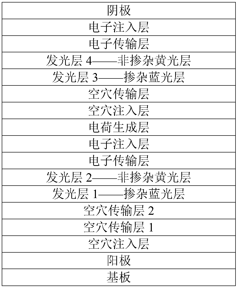
[0032] A white light series organic light-emitting device, the structure of the device is:

[0033] ITO / HAT-CN(100nm) / NPB(15nm) / TCTA(5nm) / TCTA: FIrpic(10nm, 8%) / 26DCzPPy: FIrpic(10nm, 20%) / PO-01(0.5nm) / TmPyPB(15nm ) / Bepp 2 : KBH4(10nm, 15%) / HAT-CN(100nm) / NPB(15nm) / TCTA(5nm) / TCTA: FIrpic(10nm, 8%) / 26DCzPPy: FIrpic(10nm, 20%) / PO-01( 0.5nm) / / TmPyPB(50nm) / Cs 2 CO 3 (1nm) / Al(200nm).

[0034] The structure of the device is as figure 1 Said, it is stacked by the following layers in sequence: substrate, anode, hole injection layer, hole transport layer 1, hole transport layer 2, doped blue layer, non-doped yellow light layer, electron transport layer, electron injection layer , Charge generation layer, hole injection layer, hole transport layer, doped blue light layer, non-doped yellow light layer, electron transport layer, electron injection layer, cathode.

[0035] Perform performance testing on the finished device of Example 1 obtained in this example, and the efficiency diagram is as ...

Embodiment 2

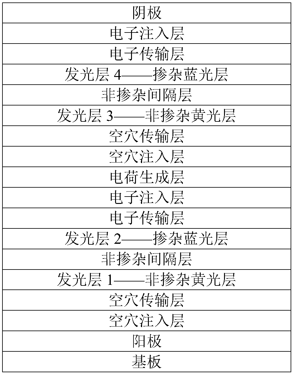
[0037] A white light series organic light-emitting device, the structure of the device is:

[0038] ITO / HAT-CN(100nm) / NPB(15nm) / PO-01(0.5nm) / m-MTDATA(3nm) / TCTA: FIrpic(10nm, 8%) / TmPyPB(15nm) / Bepp2: KBH4(10nm, 15%) / HAT-CN(100nm) / NPB(15nm) / TCTA(5nm) / PO-01(0.5nm) / Bphen(1.5nm) / TCTA: FIrpic(10nm, 8%) / TmPyPB(50nm) / Cs2CO3(1nm) / Al(200nm).

[0039] The structure of the device is as figure 2 Said, it is superimposed by the following layers in sequence: substrate, anode, hole injection layer, hole transport layer, undoped yellow light layer, undoped spacer layer, doped blue light layer, electron transport layer, electron injection layer, Charge generation layer, hole injection layer, hole transport layer, non-doped yellow light layer, non-doped spacer layer, doped blue light layer, electron transport layer, electron injection layer, cathode.

[0040] The performance of the finished device of Example 2 obtained in this example was tested, and its maximum efficiency was measured to be 63.5 cd...

Embodiment 3

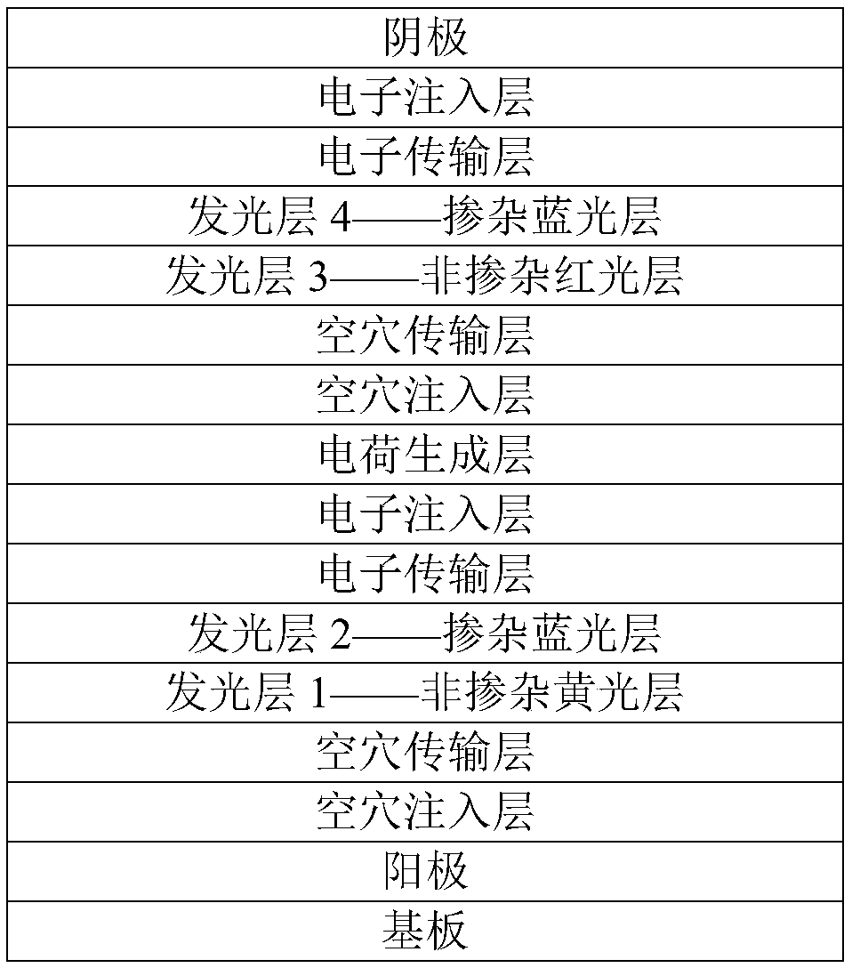
[0042] A white light series organic light-emitting device, the structure of the device is:

[0043] ITO / HAT-CN(100nm) / NPB(15nm) / PO-01(0.5nm) / TCTA: FIrpic(10nm, 8%) / TmPyPB(15nm) / Bepp 2 :KBH4(10nm, 15%) / HAT-CN(100nm) / NPB(15nm) / TCTA(5nm) / Ir(piq) 3 (0.3nm) / TCTA: FIrpic(10nm, 8%) / TmPyPB(50nm) / Cs 2 CO 3 (1nm) / Al(200nm).

[0044] The structure of the device is as image 3 Said, it consists of the following layers in sequence: substrate, anode, hole injection layer, hole transport layer, non-doped yellow light layer, doped blue layer, electron transport layer, electron injection layer, charge generation layer, hole Injection layer, hole transport layer, non-doped red light layer, doped blue light layer, electron transport layer, electron injection layer, cathode.

[0045] The performance of the finished device of Example 3 obtained in this example was tested, and its maximum efficiency was measured to be 71.8 cd / A.


PUM


Abstract

The invention discloses a white light series organic electroluminescence device. The white light series organic electroluminescence device comprises a substrate, an anode, a cathode and at least two white light luminescence unit layers positioned between the anode and the cathode, wherein the two adjacent white light luminescence unit layers are connected in series through a charge generating layer; each white light luminescence layer comprises an organic functional layer; each organic functional layer comprises at least one doped blue light layer and at least one non-doped complementary luminescence layer; and white light is obtained after light colors generated by at least one doped blue light layer and at least one non-doped complementary luminescence layer are mixed. The charge generating layer is used for connecting the white light luminescence unit layers to form the organic electroluminescence device, and the special selection and superimposed manners of the organic functional layers in the white light luminescence layers are improved, so that the structure and preparation technology of the device are greatly simplified on the basis of guaranteeing that the device has excellent luminescence property, and the device is stable in luminescence property and low in angular dependence and has wider application field.

Description

Technical field [0001] The invention relates to the technical field of organic semiconductors, in particular to an organic electroluminescence device. Background technique [0002] OLED (English full name Organic Light Emitting Diodes, meaning organic electroluminescent device, referred to as OLED) has autonomous light emission, wide viewing angle, light weight, wide temperature adaptation range, large area, full curing, flexibility, low power consumption, and response Many advantages, such as fast speed and low manufacturing cost, have important applications in the display and lighting fields, and thus have received extensive attention from academia and industry. [0003] In order to further improve the efficiency and lifespan of the device, the researchers stacked multiple independent light-emitting units, so that the same current flows through multiple different light-emitting units to emit light together to improve the brightness and efficiency of the light, forming a tandem OL...

Claims


Application Information

Patent Timeline
Patent Type & Authority Applications(China)
IPC IPC(8): H01L51/50
CPCH10K30/865H10K50/00H10K50/11H10K2101/10
Inventor 肖鹏刘佰全罗东向
Owner FOSHAN UNIVERSITY
Learn More