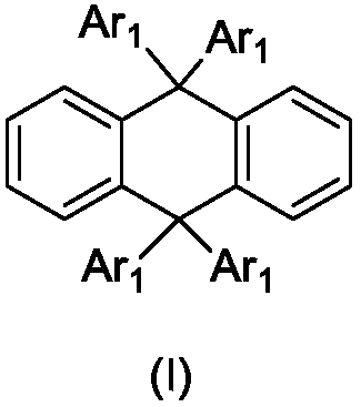
Dihydroanthracene compound containing unsaturated nitrogen heterocyclic ring, organic electroluminescent device and display device
A technology of dihydroanthracene and nitrogen heterocycle is applied in the field of display, which can solve the problems of high driving voltage and low luminous efficiency, and achieve the effect of reducing driving voltage and improving luminous efficiency.
- Summary
- Abstract
- Description
- Claims
- Application Information
AI Technical Summary
Problems solved by technology
Method used
Image

Examples
Embodiment 1
[0066] The compound of the present invention is used as the host material in the red phosphorescent OLED organic electroluminescent device, and as a comparative organic electroluminescent device, the red light host material is selected from CBP.
[0067] The structure of the organic electroluminescent device is: ITO / NPB (20nm) / red light host material (30nm): Ir(piq)3[5%] / TPBI(10nm) / Alq3(15nm) / LiF(0.5nm) / Al (150nm).
[0068] The preparation process of the organic electroluminescent device is as follows: the glass plate coated with the ITO transparent conductive layer is ultrasonically treated in a commercial cleaning agent, rinsed in deionized water, ultrasonically degreased in acetone: ethanol mixed solvent, and baked in a clean environment. Baked until completely dehydrated, cleaned with UV light and ozone, and bombarded with a beam of low-energy cations;
[0069] Place the above-mentioned glass substrate with the anode in a vacuum chamber, and evacuate to 1×10 -5 ~9×10 -3...
Embodiment 2
[0079] The compound of the present invention is used as the host material in the green phosphorescent OLED organic electroluminescent device, and as a comparative organic electroluminescent device, the green host material is respectively selected from CBP.
[0080] The structure of the organic electroluminescent device is: ITO / NPB (20nm) / green light host material (30nm): Ir(ppy)3[7%] / TPBI(10nm) / Alq3(15nm) / LiF(0.5nm) / Al (150nm).
[0081] The preparation process of the organic electroluminescent device is as follows: the glass plate coated with the ITO transparent conductive layer is ultrasonically treated in a commercial cleaning agent, rinsed in deionized water, ultrasonically degreased in acetone: ethanol mixed solvent, and baked in a clean environment. Baked until completely dehydrated, cleaned with UV light and ozone, and bombarded with a beam of low-energy cations;
[0082] Place the above-mentioned glass substrate with the anode in a vacuum chamber, and evacuate to 1×10 ...
Embodiment 3
[0091] The compound of the present invention is used as the electron transport layer in the organic electroluminescent device, and as a comparative organic electroluminescent device, the electron transport material is TAZ.
[0092] The structure of the organic electroluminescence device is: ITO / HIL02 (100nm) / NPB (40nm) / EM1 (30nm) / ETL (20nm) / LiF (0.5nm) / Al (150nm).
[0093] In the production of the organic electroluminescent device in this embodiment, a glass substrate is selected, ITO is used as the anode material, HIL02 is used as the hole injection layer, NPB is used as the hole transport layer, EM1 is used as the main material of the organic light-emitting layer, and LiF / Al is used as the electron injection layer. layer / cathode material.
[0094] The preparation process of the organic electroluminescent device in this embodiment is as follows:
[0095] The glass substrate coated with the ITO transparent conductive layer (as the anode) is ultrasonically treated in a cleanin...
PUM
 Abstract
Description
Claims
Application Information
 - Generate Ideas
- Intellectual Property
- Life Sciences
- Materials
- Tech Scout
- Unparalleled Data Quality
- Higher Quality Content
- 60% Fewer Hallucinations
Browse by: Latest US Patents, China's latest patents, Technical Efficacy Thesaurus, Application Domain, Technology Topic, Popular Technical Reports.
© 2025 PatSnap. All rights reserved.Legal|Privacy policy|Modern Slavery Act Transparency Statement|Sitemap|About US| Contact US: help@patsnap.com