Medium substrate photoetching alignment sign, alignment method and photoetching method

A technology for aligning marks and dielectric substrates, applied in microlithography exposure equipment, optics, optomechanical equipment, etc., can solve problems such as poor consistency, low alignment accuracy between reticle and dielectric substrate, and improve manufacturing accuracy and consistent effect

Active Publication Date: 2018-11-16
THE 41ST INST OF CHINA ELECTRONICS TECH GRP
View PDF3 Cites 0 Cited by
  • Summary
  • Abstract
  • Description
  • Claims
  • Application Information

AI Technical Summary

Problems solved by technology

[0007] The invention proposes a photolithographic alignment method for a dielectric substrate, which solves the problem of low alignment accuracy and poor

Method used


Image

  • Medium substrate photoetching alignment sign, alignment method and photoetching method
  • Medium substrate photoetching alignment sign, alignment method and photoetching method
  • Medium substrate photoetching alignment sign, alignment method and photoetching method

Examples


Embodiment Construction

[0038] The following will clearly and completely describe the technical solutions in the embodiments of the present invention with reference to the accompanying drawings in the embodiments of the present invention. Obviously, the described embodiments are only some, not all, embodiments of the present invention. Based on the embodiments of the present invention, all other embodiments obtained by persons of ordinary skill in the art without making creative efforts belong to the protection scope of the present invention.

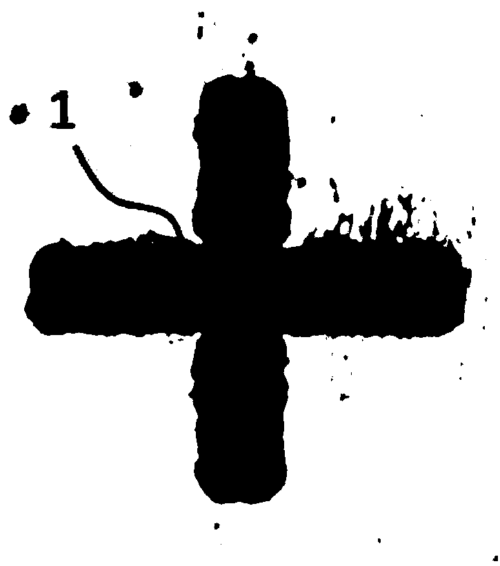
[0039] The traditional "ten" alignment mark runs through the front and back of the dielectric substrate. There is no center line when viewed in the eyepiece of the lithography machine, and it can only be aligned by relying on the unclear boundary line of the image. In the present invention, the "ten" word alignment mark on the laser processing medium substrate is only processed once, and a clear center line can be formed in the eyepiece of the lithography machi...


PUM


Abstract

The invention puts forward a medium substrate photoetching alignment sign, which is cross-shaped alignment sign processed by a laser machine, and a processing number is 1 time; the centers of the horizontal line and the vertical line of the cross-shaped alignment sign are respectively provided with a center line of which the relative edge is brighter; the cross-shaped alignment sign is arranged onthe edge of the medium substrate. When the cross-shaped alignment sign on the medium substrate is subjected to laser processing, the cross-shaped alignment sign is only processed for one time, a clear center line can be formed in the eyepiece of the lithography machine and is caused to be aligned with the center line of the cross-shaped alignment sign on a masking plate, and the accuracy of manufacture and the consistency of a film circuit are improved.

Description

technical field [0001] The invention relates to the technical field of thin film circuits, in particular to a dielectric substrate photolithography alignment mark, a dielectric substrate photolithography alignment method, and a thin film circuit photolithography method. Background technique [0002] In recent years, with the rapid development of microwave communication, microwave measurement and other fields of technology, ultra-miniature microwave devices are constantly coming out, and higher and higher requirements are put forward for microwave hybrid integrated circuits in terms of precision and integration. [0003] Due to the high operating frequency of the microwave hybrid integrated circuit, the high dimensional accuracy of the signal transmission line is required, so the circuit substrate is generally made of thin film technology, mainly including drilling, cleaning, vacuum coating, photolithography, electroplating and other processes. For thin film circuits containi...

Claims


Application Information

Patent Timeline
IPC IPC(8): G03F7/20G03F9/00
CPCG03F7/2002G03F7/70025G03F9/7019G03F9/708
Inventor 宋振国王斌路波赵习智
Owner THE 41ST INST OF CHINA ELECTRONICS TECH GRP
Why Eureka
Try Eureka