Bump element of focal plane array and preparation method of bump element

A focal plane array and bump technology, applied in the field of focal plane array, can solve the problems of poor electrical connection, easy lateral slip size of bumps, uneven size, etc. Effect

Inactive Publication Date: 2018-11-16
WUHAN GAOXIN TECH
View PDF8 Cites 2 Cited by
  • Summary
  • Abstract
  • Description
  • Claims
  • Application Information

AI Technical Summary

Problems solved by technology

[0004] The purpose of the present invention is to provide a focal plane array bump element and its preparation method, which is intended to solv

Method used


Image

  • Bump element of focal plane array and preparation method of bump element
  • Bump element of focal plane array and preparation method of bump element
  • Bump element of focal plane array and preparation method of bump element

Examples


Embodiment Construction

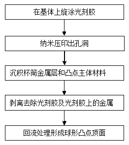
[0027] The following will clearly and completely describe the technical solutions in the embodiments of the present invention with reference to the accompanying drawings in the embodiments of the present invention. Obviously, the described embodiments are only some, not all, embodiments of the present invention. Based on the embodiments of the present invention, all other embodiments obtained by persons of ordinary skill in the art without making creative efforts belong to the protection scope of the present invention.

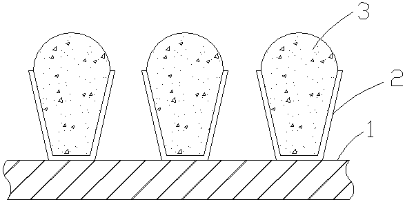
[0028] Such as figure 1 As shown, the embodiment of the present invention provides a focal plane array bump element, including a substrate 1 and a plurality of bumps on the substrate, the substrate 1 is a photosensitive material or a readout circuit, when the substrate 1 is a photosensitive material , the bump element is used to connect with the readout circuit, when the body 1 is a readout circuit, the bump element is used to connect with the photosensitive m...


PUM

PropertyMeasurementUnit
Thicknessaaaaaaaaaa
Thicknessaaaaaaaaaa

Abstract

The invention provides a bump element of a focal plane array and a preparation method of the bump element. The bump element comprises a base body and a plurality of bumps located on the base body. Each bump comprises a bump body and a cup cylinder. The diameter of the cup cylinder gradually increases from bottom to top. The bump bodies are located in the cup cylinders and fill the entire cup cylinders, and the cup cylinders are made of a metal material having electrical conductivity and certain rigidity. The bump bodies in the invention have a large top area and can ensure yield of electricalconnection. Deformation of the bump bodies mainly occurs in the lower half of the bump bodies with small diameter and weak strength, and the height compression of the bump bodies is mainly expressed in deformation of the lower parts when the flatness of photosensitive material is poor. The upper parts of the bodies can still keep a uniform radial size because of small deformation, so that uniformelectrical contact can be ensured. Also, the large top area is conducive to flip-chip bonding and avoids lateral slip. The cups are arranged on the outer side of the bump bodies, so that the bump bodies are uniform in size and the entire bumps are not easily collapsed or deformed.

Description

technical field [0001] The invention relates to the field of focal plane arrays, in particular to a focal plane array bump element and a preparation method thereof. Background technique [0002] The photoelectric signal collected by the photosensitive material part of the focal plane array is collected and processed by the readout circuit, and each pixel unit of the array must have an independent and unique output channel to ensure that the signal of each pixel point can be processed separately , and avoid crosstalk with adjacent pixel unit signals. However, the focal plane array has tens of thousands of pixels. To transmit the photoelectric signals converted by many pixels to the readout circuit, the traditional wire connection is obviously difficult to realize. In the focal plane array technology, generally Each pixel on the photosensitive material is connected to each corresponding collection unit on the readout circuit through bumps. Bumps are generally made of soft me...

Claims


Application Information

Patent Timeline
IPC IPC(8): H01L23/488H01L21/60
CPCH01L24/11H01L24/13H01L24/14H01L2224/1301H01L2224/13111H01L2224/13124H01L2224/13139H01L2224/13144H01L2224/1405
Inventor 金迎春刘斌周文洪黄立
Owner WUHAN GAOXIN TECH
Why Eureka
Try Eureka