Preparation method of three-dimensional memory and preparation method of semiconductor structure

A memory, three-dimensional technology, applied in the field of memory, can solve the problems of interface metal contamination, easy loss of the top of the memory, and poor overall shape of the channel hole.

Active Publication Date: 2018-11-16
YANGTZE MEMORY TECH CO LTD
View PDF2 Cites 33 Cited by
  • Summary
  • Abstract
  • Description
  • Claims
  • Application Information

AI Technical Summary

Problems solved by technology

[0003] In the manufacturing process of three-dimensional memory, it is necessary to make a deep channel hole. However, etching a deep channel hole will not only easily lead to poor overall shape of the channel hole, but also easily lose the top of the memory.
The existing method of setting a sacrificial layer to make a deep channel hole has problems such as interface metal contamination and high stress

Method used


Image

  • Preparation method of three-dimensional memory and preparation method of semiconductor structure
  • Preparation method of three-dimensional memory and preparation method of semiconductor structure
  • Preparation method of three-dimensional memory and preparation method of semiconductor structure

Examples


preparation example Construction

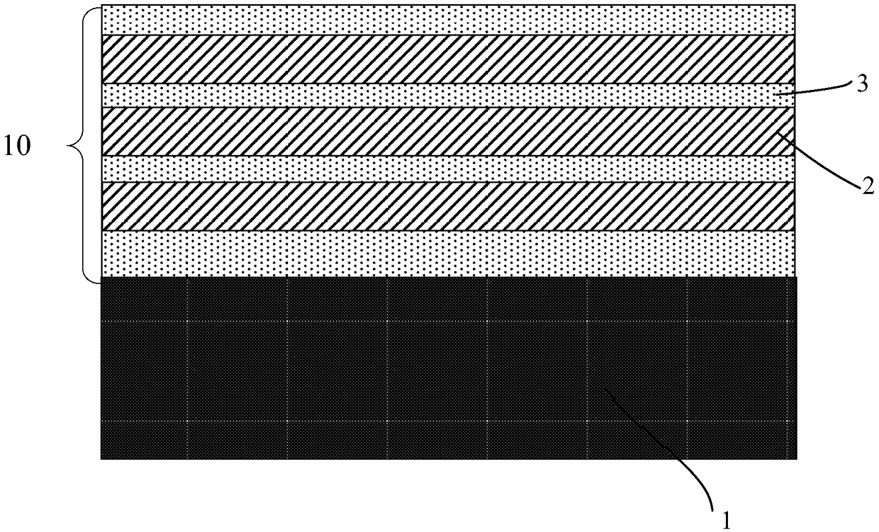
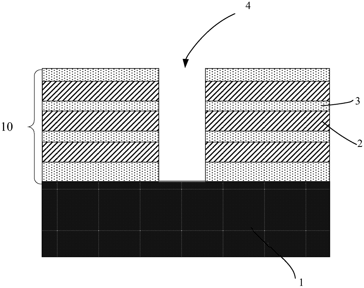
[0093] first reference figure 1 with Figure 2A to Figure 2G , an embodiment of the preparation method of the three-dimensional memory provided by the present invention is described. In the current embodiment, the method for preparing a three-dimensional memory provided by the present invention at least includes the following steps:

[0094] Step 100, refer to Figure 2A , forming a first stack 10 formed by alternately stacking the first layer 2 and the second layer 3 on the substrate 1 . In the present embodiment, the substrate 1 is made of single crystal silicon. But in other embodiments, the substrate 1 can also be made of other suitable materials, for example, in some embodiments, the material of the substrate 1 is silicon (single crystal silicon or polycrystalline silicon), germanium, silicon-on-insulator thin film ( Silicon on insulator, SOI), etc.

[0095] On the other hand, the first layer 2 and the second layer 3 may both be insulating layers, or may be an insula...


PUM

PropertyMeasurementUnit
thicknessaaaaaaaaaa
thicknessaaaaaaaaaa

Abstract

The invention discloses a preparation method of a three-dimensional memory. The preparation method comprises the steps of forming a first stack on a substrate; forming a first channel hole which vertically runs through the first stack and reaches the substrate; forming a first channel hole inner layer in the first channel hole; forming a sacrificial part in the first channel hole inner layer; forming a second stack on the first stack; forming a second channel hole which vertically runs through the second stack and reaches the sacrificial part; and removing the sacrificial part and the first channel hole inner layer. According to the preparation method of the three-dimensional memory, due to the arrangement of the sacrificial part, better stopping on a sacrificial layer can be achieved whenthe second channel hole is prepared, so that the channel hole with a relatively large depth and relatively good appearance can be formed by the first channel hole and the second channel hole.

Description

technical field [0001] The invention mainly relates to the technical field of memory, and in particular to a method for preparing a three-dimensional memory and a method for preparing a semiconductor structure. Background technique [0002] With the continued emphasis on highly integrated electronic devices, there is a continuing need for semiconductor memory devices that operate at higher speeds and lower power and have increased device densities. To this end, devices with smaller dimensions and multilayer devices with transistor cells arranged in horizontal and vertical arrays have been developed. Three-dimensional memory such as 3D NAND is an emerging type of flash memory developed by the industry. It solves the limitations of 2D or planar NAND flash memory by vertically stacking multi-layer data storage units. It has excellent precision and supports content in a smaller space. With a higher storage capacity, it can create a storage device with a storage capacity several...

Claims


Application Information

Patent Timeline
Patent Type & Authority Applications(China)
IPC IPC(8): H01L27/11551H01L27/11578
CPCH10B41/20H10B43/20
Inventor 刘峻
Owner YANGTZE MEMORY TECH CO LTD
Why Eureka
Try Eureka