Single-laser vertical cavity surface emitting laser (VCSEL) chip and fabrication method thereof

A laser and chip technology, applied in the direction of lasers, laser parts, semiconductor lasers, etc., can solve the problems of multiple beams, troublesome fitting, low power, etc., and achieve high output power, high cost of improved fitting, and simple preparation methods Effect

Inactive Publication Date: 2018-11-23
YANGZHOU CHANGELIGHT
View PDF6 Cites 1 Cited by
  • Summary
  • Abstract
  • Description
  • Claims
  • Application Information

AI Technical Summary

Problems solved by technology

[0002] At present, due to the limitation of the cavity length, the VCSEL chip only has the gain of a single resonator, so the power of a single chip is basically limited to the milliwatt level, and it is impossible to make a larger power chip, and the power is lower. Multi-chip or array chips will lead to multiple beams, and later fitting More troublesome and costly

Method used


Image

  • Single-laser vertical cavity surface emitting laser (VCSEL) chip and fabrication method thereof
  • Single-laser vertical cavity surface emitting laser (VCSEL) chip and fabrication method thereof
  • Single-laser vertical cavity surface emitting laser (VCSEL) chip and fabrication method thereof

Examples


no. 1 example

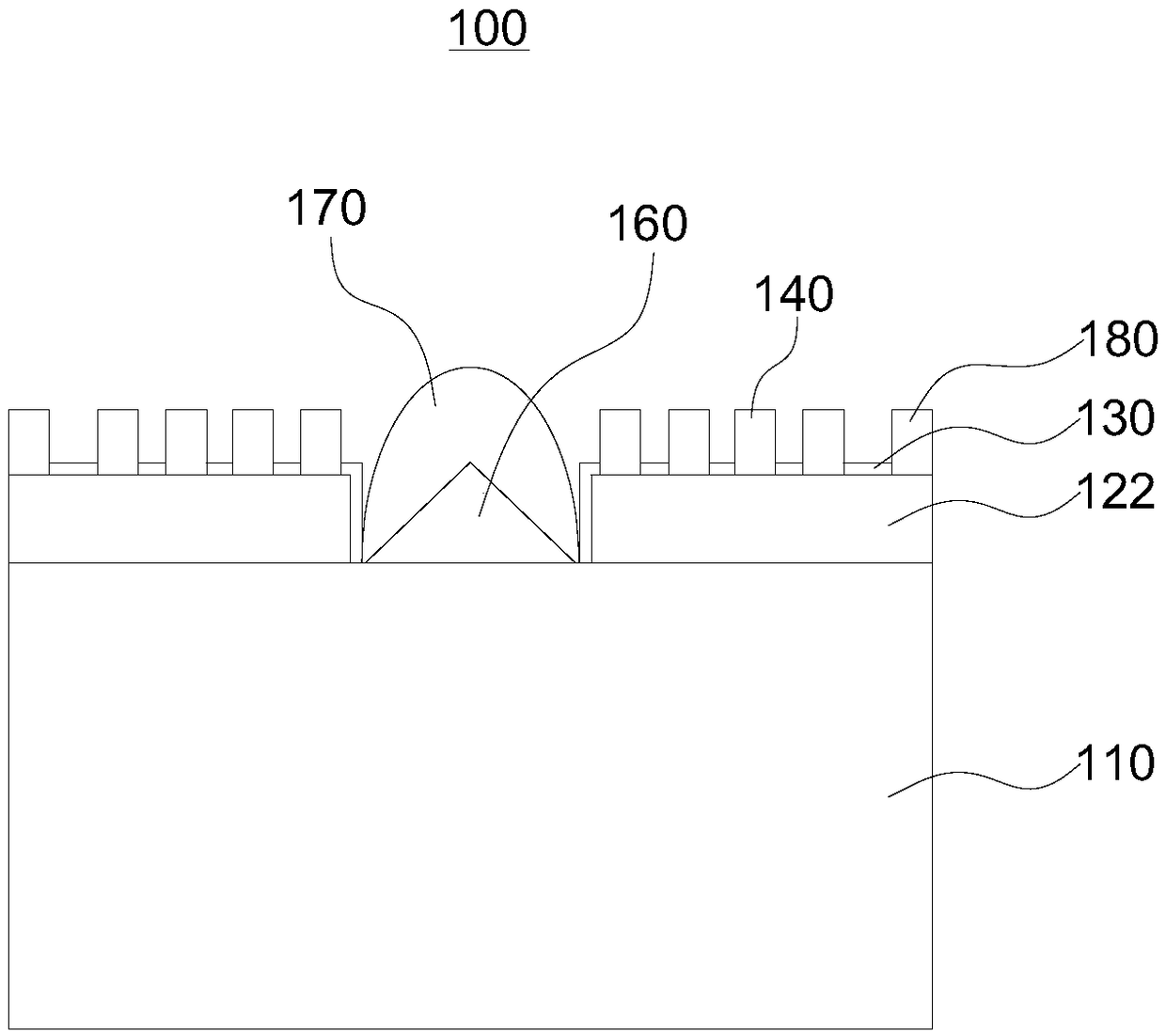
[0037] Please refer to figure 1 This embodiment provides a VCSEL chip 100 with a single laser beam, which includes a GaAs substrate 110 , an epitaxial layer 120 , a SiNx layer 130 , a grating layer 140 , a triangular mirror 160 , an epoxy resin layer 170 and an electrode 180 .

[0038] Wherein, the GaAs substrate 110 is used as the bottom layer to support the above-mentioned epitaxial layer 120 , SiNx layer 130 , grating layer 140 , triangular mirror surface 160 , epoxy resin layer 170 and electrode 180 .

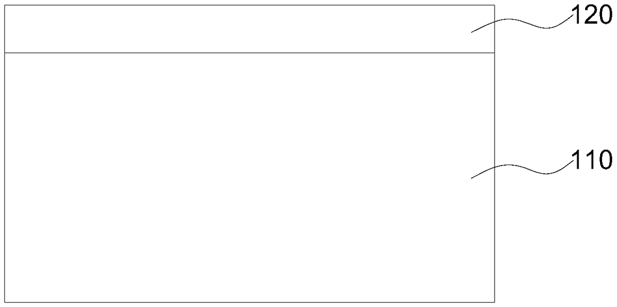
[0039] The epitaxial layer 120 is grown on the surface of the GaAs substrate 110 . The epitaxial layer 120 is etched with a groove 121 and a plurality of independent epitaxial units 122 . The plurality of epitaxial units 122 are evenly distributed along the centerline of the groove 121 . In this embodiment, the epitaxial layer 120 may be a conventional epitaxial layer 120 or a specially grown epitaxial layer 120 .

[0040] Preferably, in this embodiment, the epitaxial laye...

no. 2 example

[0056] The present embodiment provides a method for preparing a single-beam laser VCSEL chip 100, which includes the following steps:

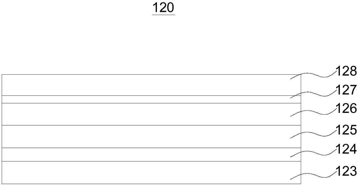
[0057] S1. In a reaction chamber with a temperature of 650-750° C. and a pressure of 40-60 mbar, the surface of the GaAs substrate 110 is first cleaned with concentrated sulfuric acid, and then the surface of the GaAs substrate 110 is cleaned with ammonia water. The surface of bottom 110 grows N-DBR layer 123, GaAs buffer layer 124, MQW layer 125 successively from bottom to top (growing MQW layer 125 is to grow a layer of AlGaAs layer on the surface of GaAs buffer layer 124 earlier, then on the surface of AlGaAs layer A layer of AlAs layer is grown, the overlapping AlGaAs layer and AlAs layer form a pair of composite layers, and then AlGaAs layer and AlAs layer are alternately grown on the surface of the AlAs layer to form 35-40 pairs of composite layers, and 35-40 pairs of composite layers are used as MQW layer 125), Al0.98Ga0.02As layer 126,...

no. 3 example

[0066] The present embodiment provides a method for preparing a single-beam laser VCSEL chip 100, which includes the following steps:

[0067] S1. Growing an epitaxial layer 120 on the surface of the GaAs substrate 110 in a reaction chamber with a temperature of 650-750° C. and a pressure of 40-60 mbar;

[0068] S2. Perform patterned photolithography on the epitaxial layer 120, etch to form a groove 121 and a plurality of mutually independent epitaxial units 122, and the plurality of epitaxial units 122 are evenly distributed along the centerline of the groove 121;

[0069] S3, depositing a SiNx layer 130 on the surface of the epitaxial unit 122;

[0070] S4. Fabricate a grating layer 140 on the surface of the SiNx layer 130 and make the diffraction direction of the grating proceed along the horizontal direction of the GaAs substrate 110;

[0071] S5. Perform patterned photolithography in the groove 121, deposit Ag and then peel off, and then repeat the deposition on the form...


PUM


Abstract

The invention relates to the field of a vertical cavity surface emitting laser (VCSEL) chip, and provides a single-laser VCSEL chip and a fabrication method thereof. The chip comprises a GaAs substrate, an epitaxial layer, a SiNx layer, a grating layer, a triangular mirror surface, an epoxy resin layer and an electrode, wherein the epitaxial layer is grown on a surface of the GaAs substrate, a groove and a plurality of epitaxial units independent to one another are etched in the epitaxial layer, the plurality of epitaxial units are uniformly arranged along a central line of the groove, the SiNx layer is deposited on surfaces of the plurality of epitaxial units, the grating layer is limited on a surface of the SiNx layer, the triangular mirror surface is arranged in the groove, the surrounding of the triangular mirror surface is filled with the epoxy resin layer, and the electrode is connected to the surface of the SiNx layer. By the chip, light emitted from the plurality of epitaxial units can be gathered to a beam of laser, so that the light giving-out power of the single-laser VCSEL chip is high. The fabrication method is simple, the light of the obtained chip can be gathered toform the beam of laser, and the light giving-out power is high.

Description

technical field [0001] The invention relates to the field of VCSEL chips, in particular to a single-beam laser VCSEL chip and a preparation method thereof. Background technique [0002] At present, due to the limitation of the cavity length, the VCSEL chip only has the gain of a single resonant cavity, so the power of a single chip is basically limited to the milliwatt level, and it is impossible to make a larger power chip, and the power is low. Multi-chip or array chips will lead to multiple beams, and later fitting More troublesome, higher cost. Contents of the invention [0003] The object of the present invention includes, for example, providing a VCSEL chip with a single laser beam, whose light can be converged into a laser beam with high light output power. [0004] The object of the present invention also includes providing a method for preparing a VCSEL chip with a single laser beam. The preparation method is simple, and the obtained VCSEL chip with a single lase...

Claims


Application Information

Patent Timeline
Patent Type & Authority Applications(China)
IPC IPC(8): H01S5/183
CPCH01S5/18308H01S5/18361
Inventor 贾钊赵炆兼马祥柱张国庆陈凯轩
Owner YANGZHOU CHANGELIGHT
Why Eureka
Try Eureka