VCSEL chip improving laser gain and preparation method thereof

A laser gain and chip technology, which is applied to lasers, laser components, semiconductor lasers, etc., can solve the problems of resonant cavity length, low gain, low light power, etc., and achieve the effect of increasing cavity length, increasing gain, and increasing power

Pending Publication Date: 2018-11-23
XIAMEN QIANZHAO SEMICON TECH CO LTD
View PDF7 Cites 3 Cited by
  • Summary
  • Abstract
  • Description
  • Claims
  • Application Information

AI Technical Summary

Problems solved by technology

[0004] In this VCSEL chip, due to the low cavity length gain of the re

Method used


Image

  • VCSEL chip improving laser gain and preparation method thereof
  • VCSEL chip improving laser gain and preparation method thereof
  • VCSEL chip improving laser gain and preparation method thereof

Examples


Embodiment Construction

[0039] The following will clearly and completely describe the technical solutions in the embodiments of the application with reference to the drawings in the embodiments of the application. Apparently, the described embodiments are only some of the embodiments of the application, not all of them. Based on the embodiments in this application, all other embodiments obtained by persons of ordinary skill in the art without making creative efforts belong to the scope of protection of this application.

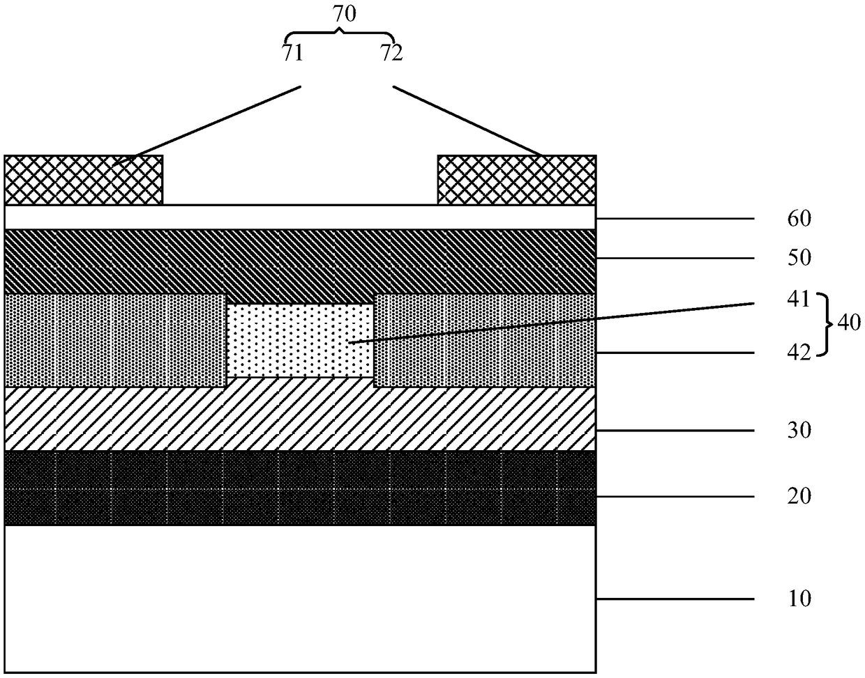
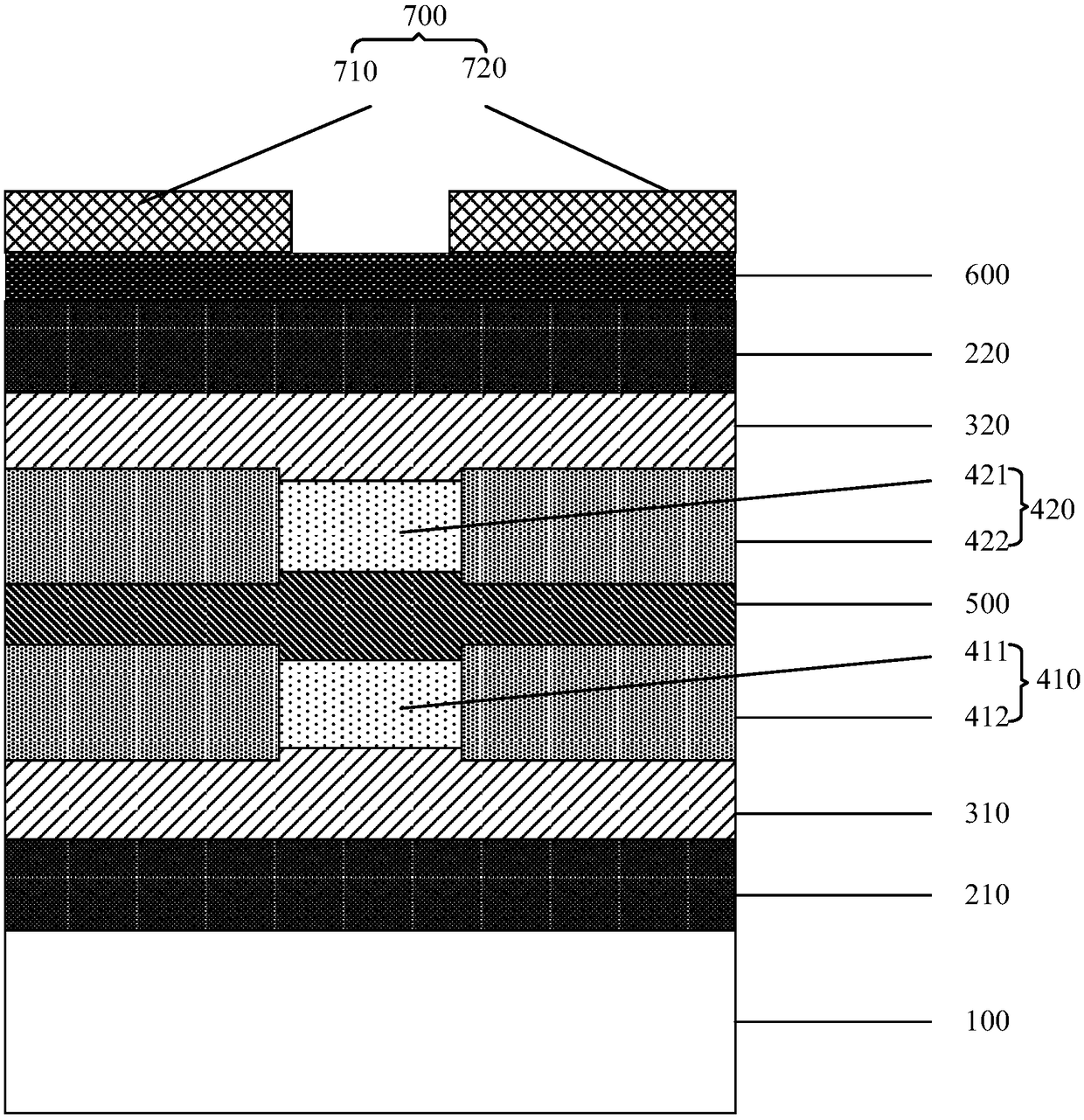
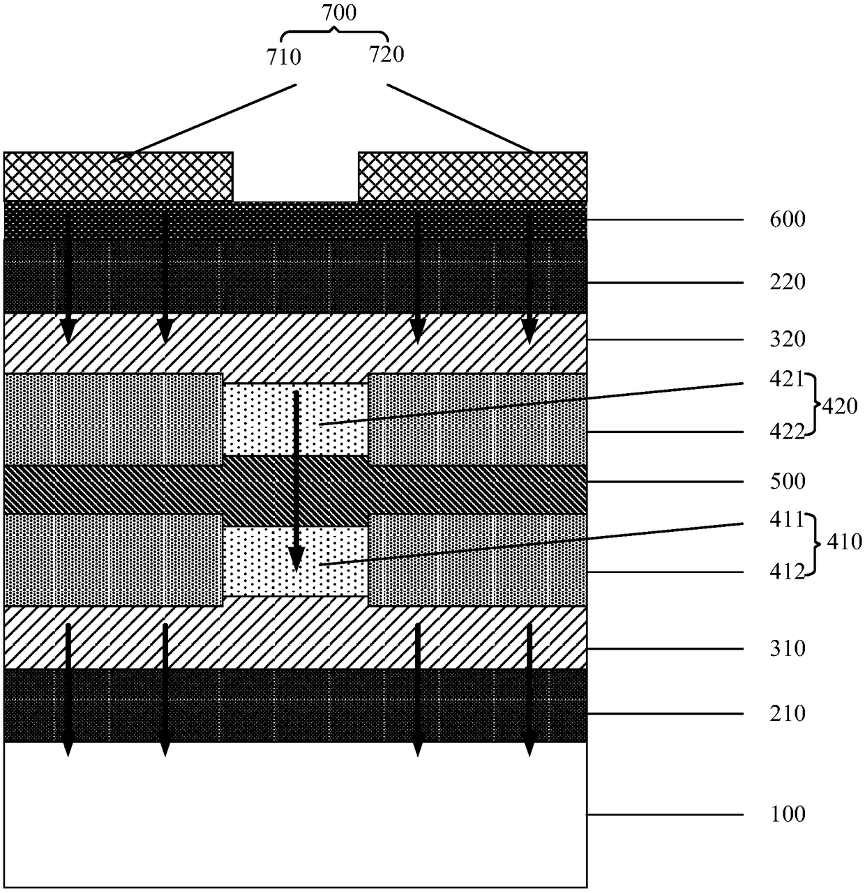
[0040] The embodiment of the present application provides a VCSEL chip for improving laser gain, such as figure 2 shown, including:

[0041] substrate 100;

[0042] An epitaxial structure on the substrate 100, the epitaxial structure includes a first-type cladding layer 310, a first confinement layer 410, a quantum well layer 500, and a second confinement layer that are sequentially stacked on the surface of the substrate 100 420, the second-type cladding layer 320 and the electr...


PUM


Abstract

The invention discloses a VCSEL chip for improving laser gain and a preparation method thereof. In an epitaxial structure of the VCSEL chip for increasing laser gain, a first type cladding layer, a first limit layer, a quantum well layer, a second limit layer and a second type cladding layer form a resonant cavity structure. In this way, the cavity length of the resonant cavity structure of the VCSEL chip is increased, so the gain of the resonant cavity structure to light generated by the quantum well layer is increased and the power of emitted light of the VCSEL chip is increased. Moreover, the existence of the first limit layer and the second limit layer enables currents of an electrode structure transmitted to the quantum well layer can still be converged by the first limit layer and the second limit layer, thereby realizing centralized injection of high currents into the quantum well layer and ensuring basic functions of the VCSEL chip.

Description

technical field [0001] The present application relates to the field of semiconductor technology, and more specifically, relates to a VCSEL chip for increasing laser gain and a preparation method thereof. Background technique [0002] Vertical cavity surface emitting laser (Vertical Cavity Surface Emitting Laser) chip, also known as VCSEL chip, is a laser emitting chip based on gallium arsenide semiconductor material, with small size, circular output spot, single longitudinal mode output, threshold current Small size, low price, easy integration into a large-area array, etc., are widely used in optical communication, optical interconnection, optical storage and other fields. [0003] The cross-sectional structure reference of the VCSEL chip in the prior art figure 1 , mainly including a gallium arsenide substrate 10 and an N-type DBR20 (Distributed Bragg Reflection, distributed Bragg reflector), a quantum well layer 30, a confinement layer 40, a P-type DBR50, and an arsenic ...

Claims


Application Information

Patent Timeline
IPC IPC(8): H01S5/183
CPCH01S5/18308H01S5/18361
Inventor 彭钰仁贾钊许晏铭洪来荣陈为民陈进顺翁妹芝张坤铭朱鸿根陈伟明许勇辉郭河
Owner XIAMEN QIANZHAO SEMICON TECH CO LTD
Why Eureka
Try Eureka