Conductive adhesive and circuit board bonding method

A conductive adhesive and circuit board technology, which is applied in the direction of assembling printed circuits, circuit covers, and printed circuits with electrical components, and can solve problems such as uneven distribution of conductive particles, narrow horizontal spacing of conductive particles, and short circuits.

Inactive Publication Date: 2018-11-23
WUHAN CHINA STAR OPTOELECTRONICS SEMICON DISPLAY TECH CO LTD
View PDF4 Cites 12 Cited by
  • Summary
  • Abstract
  • Description
  • Claims
  • Application Information

AI Technical Summary

Problems solved by technology

[0006] The invention provides a conductive adhesive and a bonding method for a circuit board to solve the problem of the uneven distribution of local conductive particles in the existing anisotropic conductive adhesive and the narrow horizontal spacing of the conductive particles leading to a short circuit, which in turn leads to the cost of the conductive adhesive. higher question

Method used


Image

  • Conductive adhesive and circuit board bonding method
  • Conductive adhesive and circuit board bonding method
  • Conductive adhesive and circuit board bonding method

Examples


Embodiment Construction

[0033] The following descriptions of the various embodiments refer to the accompanying drawings to illustrate specific embodiments in which the invention may be practiced. The directional terms mentioned in the present invention, such as [top], [bottom], [front], [back], [left], [right], [inside], [outside], [side], etc., are only for reference The orientation of the attached schema. Therefore, the directional terms used are used to illustrate and understand the present invention, but not to limit the present invention. In the figures, structurally similar elements are denoted by the same reference numerals.

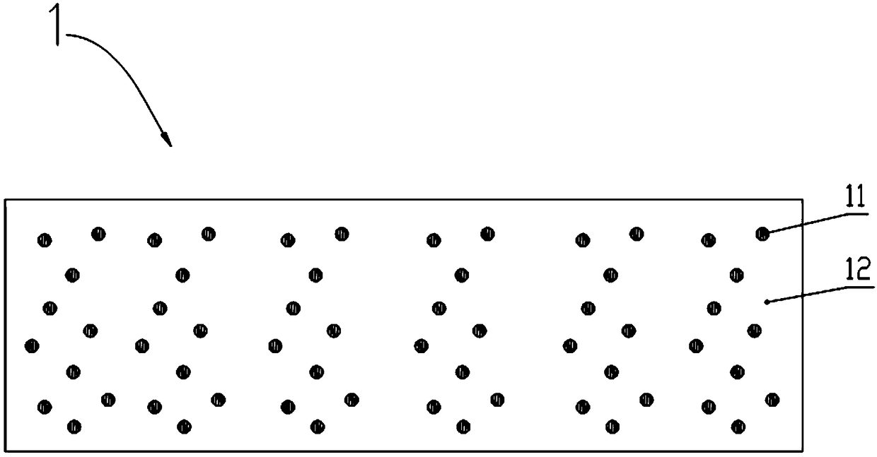
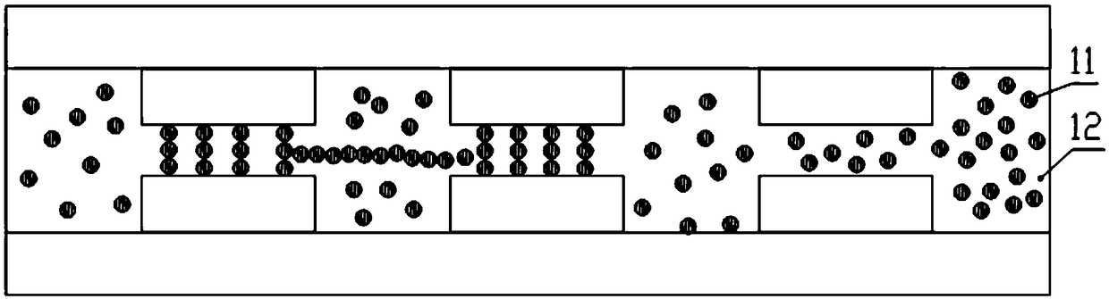
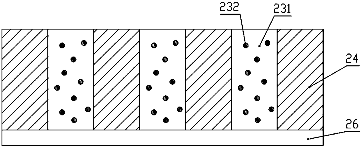
[0034] The invention aims at the problem that in the existing anisotropic conductive adhesive, due to the uneven distribution of local conductive particles, the horizontal spacing of the conductive particles is too narrow, resulting in a short circuit, which further leads to the problem of high cost of the conductive adhesive. A conductive adhesive and a bonding method...


PUM


Abstract

The invention provides a conductive adhesive and circuit board bonding method, which comprises a substrate, an insulating portion and a conducting portion formed on the surface of the substrate. The insulating portion comprises insulating rubber retaining walls spaced apart in the same direction. The conductive portion is a conductive adhesive, and the conductive adhesive is filled in a space between the adjacent insulating rubber retaining walls. According to the conductive adhesive and circuit board bonding method, the longitudinal conduction and the lateral cutting of the conductive adhesive are realized by preparing the conductive portion and the insulating portion in steps in the conductive adhesive, uniform distribution of the conductive particles can be guaranteed, and the manufacturing costs of the conductive adhesive can be reduced.

Description

technical field [0001] The invention relates to the technical field of display panel manufacturing, in particular to a conductive adhesive and a bonding method for a circuit board. Background technique [0002] With the development of society, Liquid Crystal Display (LCD for short) is gradually unable to meet users' requirements on the portability of display panels. Organic Light-Emitting Diode (OLED for short) will become a new growth point of the future display industry, which can meet the market's high requirements for mobile and portable products. [0003] In OLED technology, the bonding process plays a very important role in the entire module process, and the quality of the bonding process directly affects the display effect of the screen. Usually, the poor bonding process may cause short circuit of the display panel circuit, display offset, parts falling off, etc., which will lead to bright and dark spots, bright and dark lines, uneven display and increased black scre...

Claims


Application Information

Patent Timeline
Patent Type & Authority Applications(China)
IPC IPC(8): H05K3/32
CPCH05K3/323H05K2201/10136C09J9/02C09J7/35C09J2301/408C08K2201/001C09J2463/00C09J2467/00C09J2461/00C09J2203/326C09J2301/204H05K3/321H05K2201/0116H05K2201/0133H05K3/36H05K3/0073H05K3/1258H05K2203/1476C09J2465/00H05K3/0023
Inventor 高司恒谭金龙
Owner WUHAN CHINA STAR OPTOELECTRONICS SEMICON DISPLAY TECH CO LTD
Why Eureka
Try Eureka