
Method for Printing Circuits with Uniform Metal Droplets

A metal droplet and uniform technology, applied to other manufacturing equipment/tools, turbines, engine components, etc., can solve the problems of poor practicability, achieve good practicability, meet the needs of bonding strength, and achieve the effect of low-cost short-process printing

Active Publication Date: 2021-05-18
NORTHWESTERN POLYTECHNICAL UNIV
View PDF3 Cites 0 Cited by
  • Summary
  • Abstract
  • Description
  • Claims
  • Application Information

AI Technical Summary

Problems solved by technology

[0004] In order to overcome the shortcomings of the poor practicability of the existing microelectronic circuit manufacturing methods, the present invention provides a method for printing circuits with uniform metal droplets

Method used


Image

  • Method for Printing Circuits with Uniform Metal Droplets
  • Method for Printing Circuits with Uniform Metal Droplets
  • Method for Printing Circuits with Uniform Metal Droplets

Examples


Embodiment 1

[0026] Example 1. Printing of electronic circuits on thermoplastic substrates.

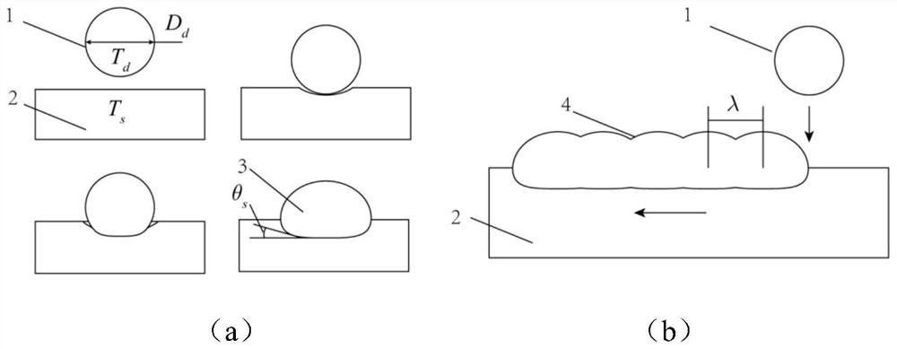
[0027] Lead-tin alloy (ZHLZn60PbA) was used as the printing material, and organic glass (polymethyl methacrylate) was used to process the thermoplastic substrate 2. First, heat the lead-tin alloy inside the crucible to 300°C-400°C, match the pressure amplitude, pulse width and frequency of the metal droplet injection, and realize the stable injection of a single uniform metal droplet 1.

[0028] in accordance with:

[0029] T d > T g (1)

[0030] ρV d C(T d -T s )>ρV 搭接 C(T d -T s )+ρV 搭接 H (2)

[0031] Calculate the temperature T of the high-temperature metal droplet 1 d with thermoplastic matrix 2 temperature T s . T d The value range is: T d =300℃~400℃, T s The value range is: T s =100°C to 200°C. The metal droplet 1 is sprayed with a diameter of about 200-500 μm, so that it is precisely positioned on the surface of the thermoplastic substrate 2 . The metal droplet 1 melts...

Embodiment 2

[0035] Example 2. Fast printing of highly conductive electronic circuits on high melting point substrates.

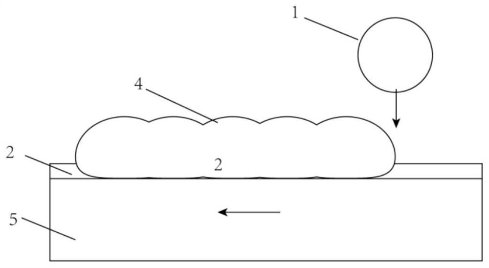
[0036] For high-melting-point insulating substrates 5 such as glass and ceramics, a thermoplastic layer 2 is firstly coated on the surface to prepare a composite substrate for printing metal droplets 1 . The gold-tin alloy (AuSn30) was used as the printing material, and the personalized circuit was directly printed on the prepared composite substrate.

[0037] in accordance with:

[0038] T d > T g (1)

[0039] ρV d C(T d -T s )>ρV 搭接 C(T d -T s )+ρV 搭接 H (2)

[0040] Calculate the temperature T of the high-temperature metal droplet 1 d with thermoplastic matrix 2 temperature T s . T d The value range is: T d =400℃~500℃, T s The value range is: T s =100°C to 200°C. Spray metal droplet 1 with a diameter of about 200-500 μm, and conduct gold-tin alloy droplet deposition test on thermoplastic substrate 2 to obtain good fusion between metal droplet 1 and ...


PUM

PropertyMeasurementUnit
diameteraaaaaaaaaa

Abstract

The invention discloses a method for printing circuits with uniform metal droplets, which is used to solve the technical problem of poor practicability of the existing microelectronic circuit manufacturing methods. The technical solution is to melt the bulk metal material supplied in the market, spray out molten metal droplets for drop-by-drop printing, and ensure the conductivity of the printed conductive circuit and the conductivity of the dense metal material through the metallurgical combination of the printed metal droplets. Sex is the same. At the same time, when the high-temperature droplets are deposited, the thermoplastic substrate is melted to form a conductive circuit embedded in the substrate at the bottom of the metal droplet, so as to meet the needs of the bonding strength of the conductive circuit, reduce the post-processing process of the circuit, and realize the low-cost and short-process printing of the circuit. Good practicality.

Description

technical field [0001] The invention relates to a method for manufacturing a microelectronic circuit, in particular to a method for printing a circuit with uniform metal droplets. Background technique [0002] With the development of electronic products in the direction of ultra-large-scale integration, digitalization, lightweight and personalization, the current research on multi-sensing microsystems and optoelectronic processes urgently needs to be able to personalize, High-efficiency wiring can greatly improve the production efficiency and precision of electronic products, save time and cost, which poses a challenge to the traditional circuit manufacturing process. The traditional circuit manufacturing process mostly adopts mask-based screen printing process, which is suitable for the production of large-scale standardized products, and it is difficult to meet the rapid manufacturing of advanced microelectronics such as 3D circuits, organic photoelectric circuits, and pho...

Claims


Application Information

Patent Timeline
Patent Type & Authority Patents(China)
IPC IPC(8): B22F3/115B22F5/00
CPCB22F3/115B22F5/00
Inventor 罗俊齐乐华赵蕾莫远兵
Owner NORTHWESTERN POLYTECHNICAL UNIV
Learn More