Optical receiving device

A light-receiving device and technology of the device, applied in the field of optical communication, can solve the problems of difficult coupling of the optical path of the photosensitive surface of the PD chip, and achieve the effect of solving the reduction of the photosensitive surface

Inactive Publication Date: 2018-11-30
GUANGXUN SCI & TECH WUHAN
View PDF5 Cites 6 Cited by
  • Summary
  • Abstract
  • Description
  • Claims
  • Application Information

AI Technical Summary

Problems solved by technology

[0005] The embodiment of the present invention provides a light-receiving device to solve the existing problem of difficulty in optical coupling caused by the reduction of the photosensitive surface of the PD chip due to the increase in the rate

Method used


Image

  • Optical receiving device
  • Optical receiving device
  • Optical receiving device

Examples


example 1

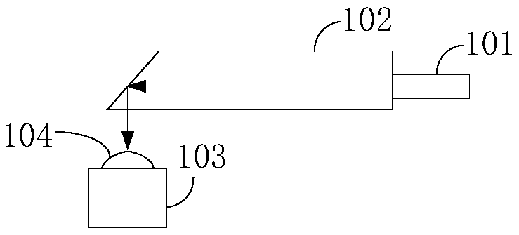
[0048] Figure 4 It is a structural schematic diagram of a light receiving device according to an embodiment of the present invention, refer to Figure 4 , an optical receiving device, including a pin 306 , an input optical fiber 101 , a waveguide chip 102 , a PD chip 103 and a transimpedance amplifier 302 . Wherein, the pin 306 is coupled to the input port of the input optical fiber 101, and the coupling port of the input optical fiber 101 is coupled to the input end face of the waveguide chip 102. Four PD chips 103 are arranged below the output end face of the waveguide chip 102, and each PD chip 103 A lens 104 is etched above the photosensitive surface for converging the optical signal emitted from the output end surface of the waveguide chip 102 and irradiating it onto the photosensitive surface of the PD chip 103 . The PD chip 103 is connected to the transimpedance amplifier 302 through gold wire bonding.

[0049] Wherein, the PD chip 103 is connected through a flip-chi...

example 2

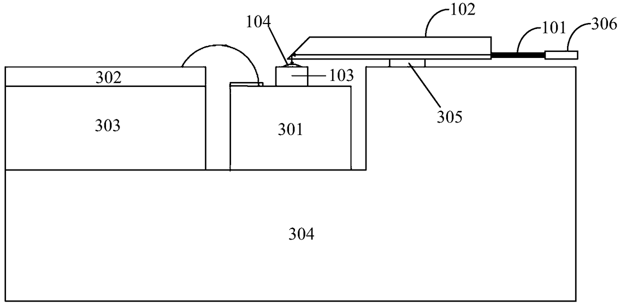
[0055] refer to image 3 , the optical signal enters the input optical fiber 101 through the ferrule, and is transmitted in the waveguide through the waveguide chip 102 until it reaches the waveguide surface of the waveguide chip 102. Since the output end surface of the waveguide chip 102 is polished to an angle of 42° with the waveguide surface, the light passes through After total reflection, it is incident on the lens 104 of the PD chip 103 directly below. After being converged by the lens 104, it is irradiated on the photosensitive surface. The optical signal irradiated on the photosensitive surface of the PD chip 103 is converted into an electrical signal by the transimpedance amplifier 302 at the rear end and amplified. . The PD chip 103 and the transimpedance amplifier 302 are cascaded with gold wire bonding metal. Since different wire lengths will introduce different parasitic inductances and capacitances, especially in high-speed devices, the receiver bandwidth will b...

example 3

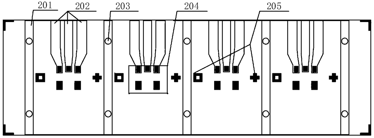
[0057] refer to figure 2 , the PD transition block 301 is provided with a ground isolation region 201 , a signal line 202 , a through hole 203 , a solder area 204 and a marking point 205 .

[0058] The back of the PD chip 103 used in this example has a deeply etched lens 104, which functions to expand the receiving area of ​​the active region and reduce the difficulty of coupling. However, compared with the conventional front-incidence PD chip 103 , the mounting process of the back-incidence PD chip 103 is more complicated. In this example, a flip-chip mounting process is developed for the back-incidence PD chip 103. In order to ensure the feasibility of the process, a special aluminum nitride transition block, namely the PD transition block 301, is used in the design. Five gold-tin solder regions 204 are preset on the PD transition block 301 , which correspond to the gold-plated region at the bottom of the PD chip 103 . When welding, heat and pressure technology is used to...


PUM


Abstract

The embodiment of the invention provides an optical receiving device comprising an input optical fiber, a waveguide chip and a plurality of PD chips. A lens is etched on the photosensitive surface ofeach PD chip; and a coupling port of the input optical fiber is bonded with the input end face of the waveguide chip in a coupled mode, the multiple PD chips are located below the output end face of the waveguide chip, and the lens of any PD chip is used for converging optical signals emitted by the output end face of the waveguide chip and irradiating the optical signals on the photosensitive surface of any PD chip. According to the optical receiving device, the area of a PD chip active area is enlarged by applying the PD chips etched with the lenses, thus the problem of difficult coupling caused by decreasing of the photosensitive surfaces of the PD chips in a high-speed state is solved, an idea is provided for meeting the optical receiving device with the higher transmission rate, and the condition is created for realizing passive coupling of the optical receiving device.

Description

technical field [0001] Embodiments of the present invention relate to the technical field of optical communication, and in particular, to an optical receiving device. Background technique [0002] With the vigorous development of the optical communication field, many medium and long-distance products are required to meet higher-speed parallel transmission methods. At present, the commercialized 25GX4 modules have only gradually entered mass production, and the market demand points to modules with higher speed requirements such as 400G. In 2016, 13 companies jointly established the QSFP-DD MSA. QSFP-DD has the same bandwidth as QSFP28. , high (undetermined length) aims to create a module with double the density, and the miniaturized package of the module poses more stringent challenges to the device. The QSFP-DD module adopts 4-channel optical path and PAM4 modulation format. [0003] From the perspective of optical receiving devices, it is very difficult to increase the ba...

Claims


Application Information

Patent Timeline
IPC IPC(8): G02B6/42
CPCG02B6/4204
Inventor 成璇璇宋琼辉胡毅
Owner GUANGXUN SCI & TECH WUHAN
Why Eureka
Try Eureka