Ultrasonic wave fingerprint recognition sensor and manufacture method thereof
A fingerprint recognition and production method technology, which is applied in character and pattern recognition, acquisition/organization of fingerprints/palmprints, instruments, etc., can solve the problems of high production cost, small penetration thickness, low resolution, etc., and achieve low production cost. , the effect of high penetration film thickness, high resolution and signal-to-noise ratio
- Summary
- Abstract
- Description
- Claims
- Application Information
AI Technical Summary
Problems solved by technology
Method used
Image

Examples
Embodiment 1
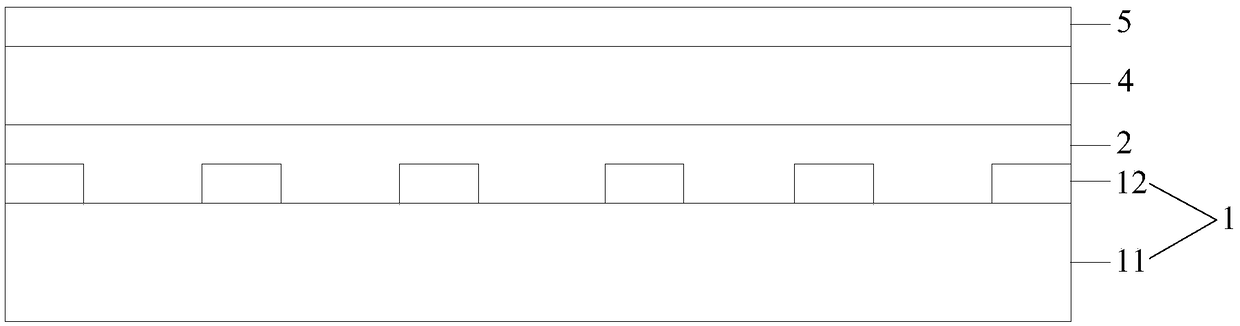
[0021] figure 2 It is a schematic structural diagram of the ultrasonic fingerprint recognition sensor provided by the first embodiment of the present invention, as figure 2 As shown, the sensor includes a CMOS backplane layer 1, a buffer layer 2, a PVDF layer 4, and an ITO transmitting electrode 5 arranged in sequence. The CMOS backplane layer 1 includes a CMOS structure 11 and an ITO receiving electrode 12. The buffer layer 2 includes SiNx, ITO The receiving electrodes 12 are embedded in the buffer layer 2 at intervals, wherein an isolation layer 3 is provided between the buffer layer 2 and the PVDF layer 4 to separate the buffer layer 2 from the PVDF 4 .
[0022] Optionally, the isolation layer 3 in this embodiment is composed of spaced columnar structures.
[0023] Optionally, the isolation layer 3 is made of inverse ITO Float metal. Further, the Float metal of the inverse ITO may be, but not limited to, Ti-Al-Ti or Al or Mo.
[0024] Specifically, the Space in the iso...
Embodiment 2
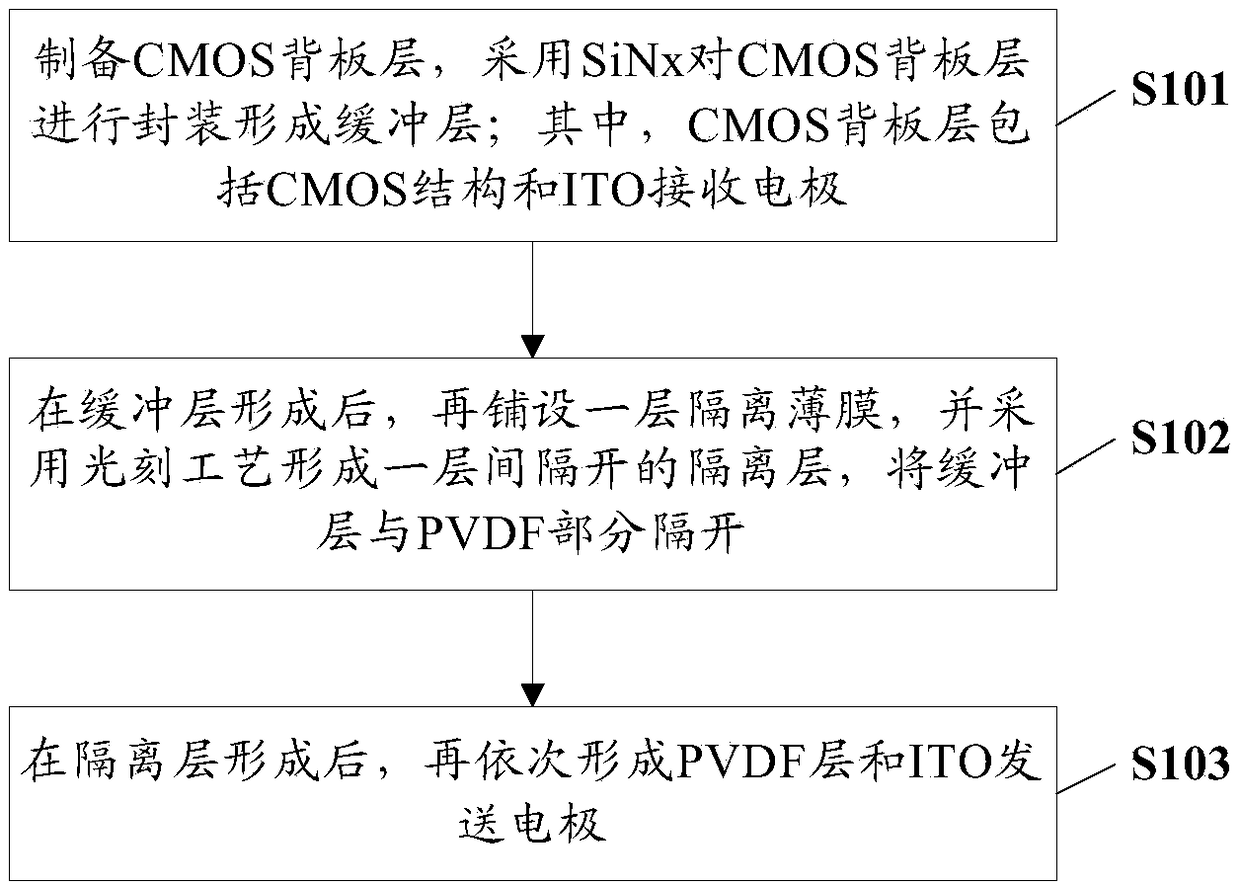
[0030] image 3 is made figure 2 The flow chart of the method of the ultrasonic fingerprint recognition sensor of the shown embodiment, as image 3 shown, including:
[0031] S101 , preparing a CMOS backplane layer, and encapsulating the CMOS backplane layer with SiNx to form a buffer layer; wherein, the CMOS backplane layer includes a CMOS structure and an ITO receiving electrode.
[0032] S102. After the buffer layer is formed, lay a layer of isolation film, and use a photolithography process to form a layer of spaced isolation layer to separate the buffer layer from the PVDF part.
[0033] Optionally, the isolation layer in this embodiment is composed of spaced columnar structures.
[0034] Optionally, the isolation layer is made of inverse ITO Float metal. Further, the Float metal of the inverse ITO may be, but not limited to, Ti-Al-Ti or Al or Mo.
[0035] Optionally, the thickness of the isolation layer is less than or equal to 1000A.
[0036] Optionally, the isol...
Embodiment 3
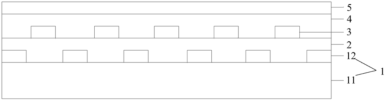
[0041] Figure 4 is a schematic structural diagram of the ultrasonic fingerprint recognition sensor provided by the second embodiment of the present invention, as Figure 4 As shown, the sensor includes a CMOS backplane layer 1, a buffer layer 2, a PVDF layer 4, and an ITO transmitting electrode 5 arranged in sequence, the CMOS backplane layer 1 includes a CMOS structure 11 and an ITO receiving electrode 12, the buffer layer 2 includes SiNx, and the ITO receiving electrode 5 The electrodes 12 are embedded in the buffer layer 2 at intervals, wherein an isolation layer 3 is provided between the buffer layer 2 and the PVDF layer 4 to completely separate the buffer layer 2 from the PVDF 4 .
[0042] Optionally, the isolation layer 3 in this embodiment is composed of a continuous structure.
[0043] Optionally, the isolation layer 3 is made of inverse ITO Float metal. Further, the Float metal of the inverse ITO may be, but not limited to, Ti-Al-Ti or Al or Mo.
[0044] Optionall...
PUM
| Property | Measurement | Unit |
|---|---|---|
| Thickness | aaaaa | aaaaa |
Abstract
Description
Claims
Application Information
 - R&D
- Intellectual Property
- Life Sciences
- Materials
- Tech Scout
- Unparalleled Data Quality
- Higher Quality Content
- 60% Fewer Hallucinations
Browse by: Latest US Patents, China's latest patents, Technical Efficacy Thesaurus, Application Domain, Technology Topic, Popular Technical Reports.
© 2025 PatSnap. All rights reserved.Legal|Privacy policy|Modern Slavery Act Transparency Statement|Sitemap|About US| Contact US: help@patsnap.com