Method for realizing transient circuit packaging structure for packaging silicon-based chip

A technology of transient circuit and packaging structure, applied in the electronic field, to achieve the effect of wide industrial prospects and simple packaging process

Active Publication Date: 2018-11-30
NO 24 RES INST OF CETC
View PDF8 Cites 2 Cited by
  • Summary
  • Abstract
  • Description
  • Claims
  • Application Information

AI Technical Summary

Problems solved by technology

However, there is no transient packaging process specifically for silicon-based chips at present. Therefore, there is an urgent need for a packaging structure realization method for transient circuits to meet the requirements that the overall packaging structure of the circuit can be completely degraded in water, and in the packaging process. Realize the transfer printing, assembly and interconnection of silicon-based chips

Method used


Image

  • Method for realizing transient circuit packaging structure for packaging silicon-based chip
  • Method for realizing transient circuit packaging structure for packaging silicon-based chip
  • Method for realizing transient circuit packaging structure for packaging silicon-based chip

Examples


Embodiment Construction

[0028] Embodiments of the present invention are described below through specific examples, and those skilled in the art can easily understand other advantages and effects of the present invention from the content disclosed in this specification. The present invention can also be implemented or applied through other different specific implementation modes, and various modifications or changes can be made to the details in this specification based on different viewpoints and applications without departing from the spirit of the present invention. It should be noted that, in the case of no conflict, the following embodiments and features in the embodiments can be combined with each other.

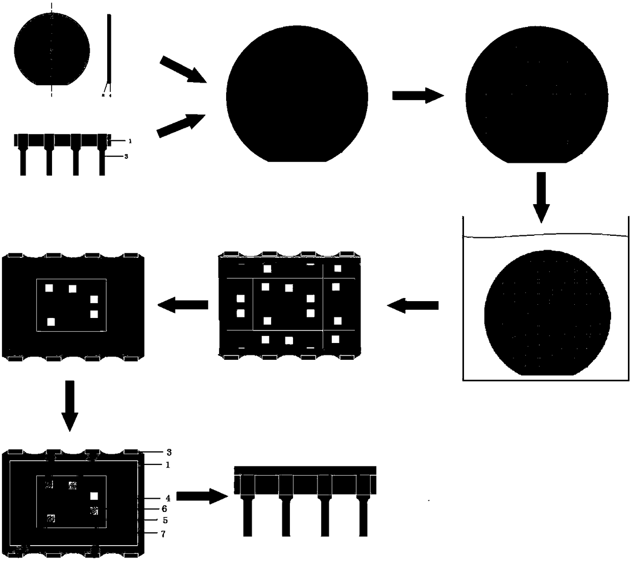
[0029] It should be noted that the diagrams provided in the following embodiments are only schematically illustrating the basic ideas of the present invention, and only the components related to the present invention are shown in the diagrams rather than the number, shape and shape of the compo...


PUM

PropertyMeasurementUnit
Thicknessaaaaaaaaaa
Thicknessaaaaaaaaaa
Thicknessaaaaaaaaaa

Abstract

The invention provides a method for realizing a transient circuit packaging structure for packaging a silicon-based chip. The method for realizing a transient circuit packaging structure for packagingthe silicon-based chip comprises the following steps that polyvinyl alcohol solution or water is arranged between a shell and a thin silicon chip to be packaged in a coating mode; a polyvinyl alcoholtube shell adheres to the silicon-based chip; drying and baking treatment are carried out to form an integral wafer structure; and stripping treatment is carried out on the whole wafer structure to strip the silicon-based chip adhered to the polyethylene alcohol tube shell from the silicon-based supporting wafer, and then an electrical interconnection channel is established. The full circuit packaging structure can be degraded in water, all packaging materials do not involve toxic and non-degradable materials, and environment protection is achieved. The packaging process is relatively simpleand can be repeatedly realized under the prior art conditions. The packaging structure can prepare tube shells with different sizes and leading-out end structures through a jig, and can realize plug-in and plug-out interchange with an existing integrated circuit electronic device. The method for realizing a transient circuit packaging structure for packaging the silicon-based chip overturns the traditional electronic industry and has a wide industrial prospect.

Description

technical field [0001] The invention relates to the field of electronic technology, in particular to a method for realizing a transient circuit packaging structure for packaging silicon-based chips. Background technique [0002] In order to function stably, current mainstream electronic devices are usually made of non-degradable, very stable, and possibly even toxic (such as gallium arsenide) substrate materials and electronic components. With the development of electronic preparation technology, serious environmental pollution has become one of the important problems threatening human society. Therefore, it is of great significance to develop electronic devices such as environmentally friendly, low-toxicity and safe electronic devices that can replace traditional electronic products. [0003] Transient electronic technology is a revolutionary breakthrough technology of electronic technology newly proposed in recent years. It is a technology that can solve the environmental...

Claims


Application Information

Patent Timeline
IPC IPC(8): H01L21/56H01L23/488
CPCH01L21/568H01L23/488
Inventor 郑旭肖玲廖希异谢东王涛周玉明陈仙袁俊张培健
Owner NO 24 RES INST OF CETC
Why Eureka
Try Eureka