Electro-acoustic effect-based in-situ detection method and device for electron beam additive manufacturing

A technology of additive manufacturing and in-situ inspection, applied in the field of additive manufacturing, can solve the problems of difficulty in meeting the requirements of precision and resolution, increase in equipment cost and complexity, and achieve improved cost and complexity, small size, and simple structure. Effect

Inactive Publication Date: 2018-12-14
INST OF ELECTRICAL ENG CHINESE ACAD OF SCI
View PDF2 Cites 6 Cited by
  • Summary
  • Abstract
  • Description
  • Claims
  • Application Information

AI Technical Summary

Problems solved by technology

However, for electron beam additive manufacturing, if X-ray CT detection technology is used, large-sized metal samples require extremely strong radiation intensity, and the cost and complexity of the corresponding equipment will be greatly increased; The problem of mechanical interference between processed parts, in which it is difficult to couple the sound source and detector with the parts to be tested during the processing process, making it difficult to meet the accuracy and resolution of real-time measurement

Method used


Image

  • Electro-acoustic effect-based in-situ detection method and device for electron beam additive manufacturing
  • Electro-acoustic effect-based in-situ detection method and device for electron beam additive manufacturing
  • Electro-acoustic effect-based in-situ detection method and device for electron beam additive manufacturing

Examples


Embodiment Construction

[0034] The present invention will be further described in detail below in conjunction with the accompanying drawings and embodiments.

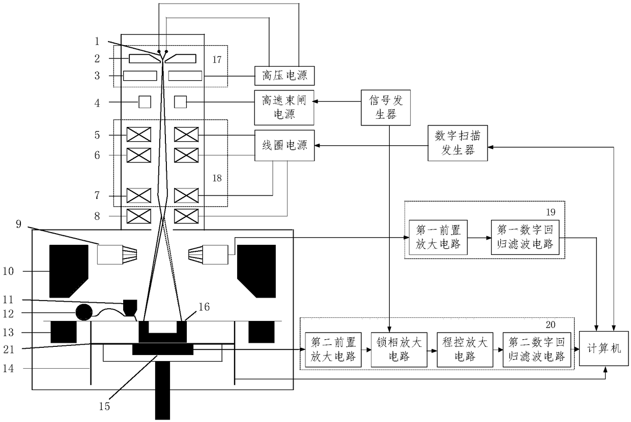
[0035] The invention provides an in-situ detection method and device for electron beam additive manufacturing based on electroacoustic effect.

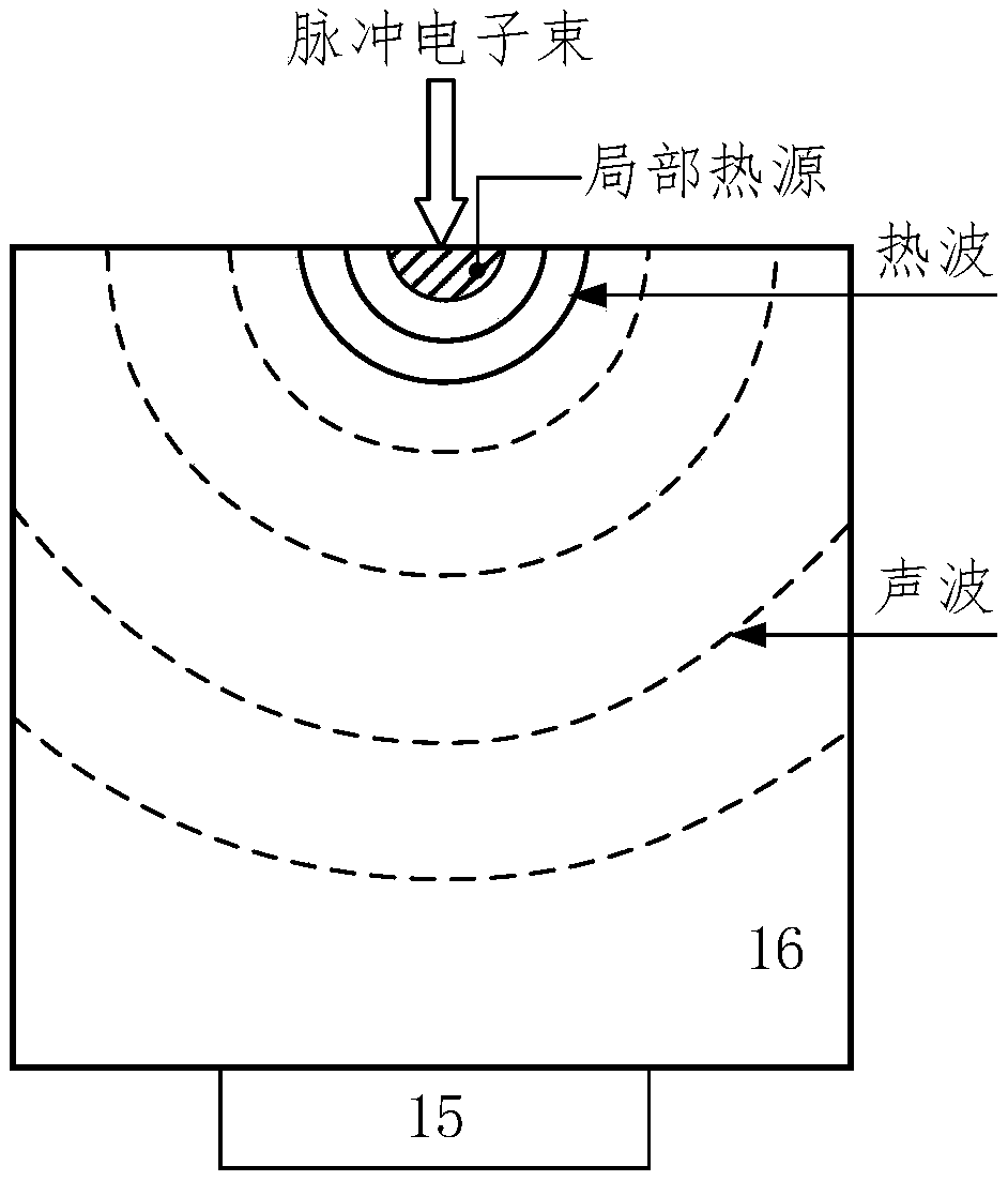
[0036] When the electron beam interacts with the material, it will generate secondary electrons, backscattered electrons, characteristic X-rays, Auger electrons, transmitted electrons and other signals, which can be used to accurately identify the characteristic information of the material surface. Among them, using secondary electrons or backscattered electrons to obtain the distribution of topographic features of the surface area of ​​the workpiece 16 is a common method in scanning electron microscopy (SEM) (reference [3] Lin Feng, Yan Yongnian, Yan Zhangong, etc., an electron beam selected area synchronous Sintering process and three-dimensional layered manufacturing equipment [P], Chinese patent, ...


PUM


Abstract

The invention discloses an electro-acoustic effect-based in-situ detection method and device for electron beam additive manufacturing and belongs to the technical field of additive manufacturing. Surface topography characteristics of a workpiece are obtained after a pulsed electron beam interacts with the surface of the workpiece, meanwhile, a heat wave generated after the pulsed electron beam interacts with the surface of the workpiece is conducted towards the inside of the workpiece along the surface of the workpiece to form an acoustic wave, and the acoustic wave is received to achieve electro-acoustic signal detection through adding a transducer to the lower part of the workpiece, thereby obtaining internal layered structure characteristics of the workpiece. The detection device comprises a secondary electron or backscattered electron detection system, an electro-acoustic signal detection system, a signal generator and a digital scanning generator. The method and the device disclosed by the invention are used for detecting the surface topography characteristics and the internal layered structure characteristics of the workpiece in the additive manufacturing process and monitoring the manufacturing quality; the detection device is small in size, simple in structure and good in coupling property; and the cost and the complexity are not additionally increased.

Description

technical field [0001] The invention belongs to the technical field of additive manufacturing, and in particular relates to an in-situ detection method and device for electron beam additive manufacturing based on electroacoustic effects. Background technique [0002] Additive manufacturing technology, also known as 3D printing technology, uses a computer to design a three-dimensional digital model, uses high-energy beams to fuse materials into one, and realizes the manufacturing of physical parts through layer-by-layer accumulation. It is a revolutionary green intelligent manufacturing technology. The additive manufacturing technology using electron beam as energy source has the advantages of high energy density, fast scanning speed, wide range of processing materials, no reflection, no pollution in vacuum environment and relatively low operating cost. It not only has high raw material utilization rate, but also can manufacture Structural components with complex shapes have ...

Claims


Application Information

Patent Timeline
Patent Type & Authority Applications(China)
IPC IPC(8): G01N23/203G01N23/2251G01N29/04
CPCG01N23/203G01N23/2251G01N29/045
Inventor 赵伟霞刘俊标马玉田殷伯华韩立牛耕
Owner INST OF ELECTRICAL ENG CHINESE ACAD OF SCI
Why Eureka
Try Eureka