LED epitaxial structure and preparation method thereof

An epitaxial structure and superlattice technology, which is applied in the direction of electrical components, circuits, semiconductor devices, etc., can solve the problems of LED luminous efficiency decline, achieve the effect of reducing the conduction band energy level drop and reducing non-radiative recombination

Inactive Publication Date: 2018-12-14
FOCUS LIGHTINGS SCI & TECH
View PDF7 Cites 6 Cited by
  • Summary
  • Abstract
  • Description
  • Claims
  • Application Information

AI Technical Summary

Problems solved by technology

[0003] In the prior art, the LED structure directly grows the P-type hole injection layer and the P-type GaN layer after the growth of the multi-quantum well light-emitting layer, wherein the Mg, Zn, etc. in the P-type hole injection layer an

Method used


Image

  • LED epitaxial structure and preparation method thereof
  • LED epitaxial structure and preparation method thereof
  • LED epitaxial structure and preparation method thereof

Examples


Example Embodiment

[0037] The present invention will be described in detail below in conjunction with the specific embodiments shown in the drawings. However, these embodiments do not limit the present invention, and the structural, method, or functional changes made by those skilled in the art based on these embodiments are all included in the protection scope of the present invention.
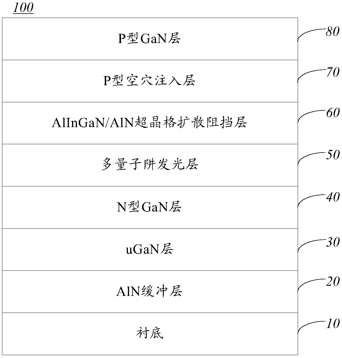
[0038] Such as figure 1 Shown is a schematic diagram of an LED epitaxial structure 100 according to an embodiment of the present invention.

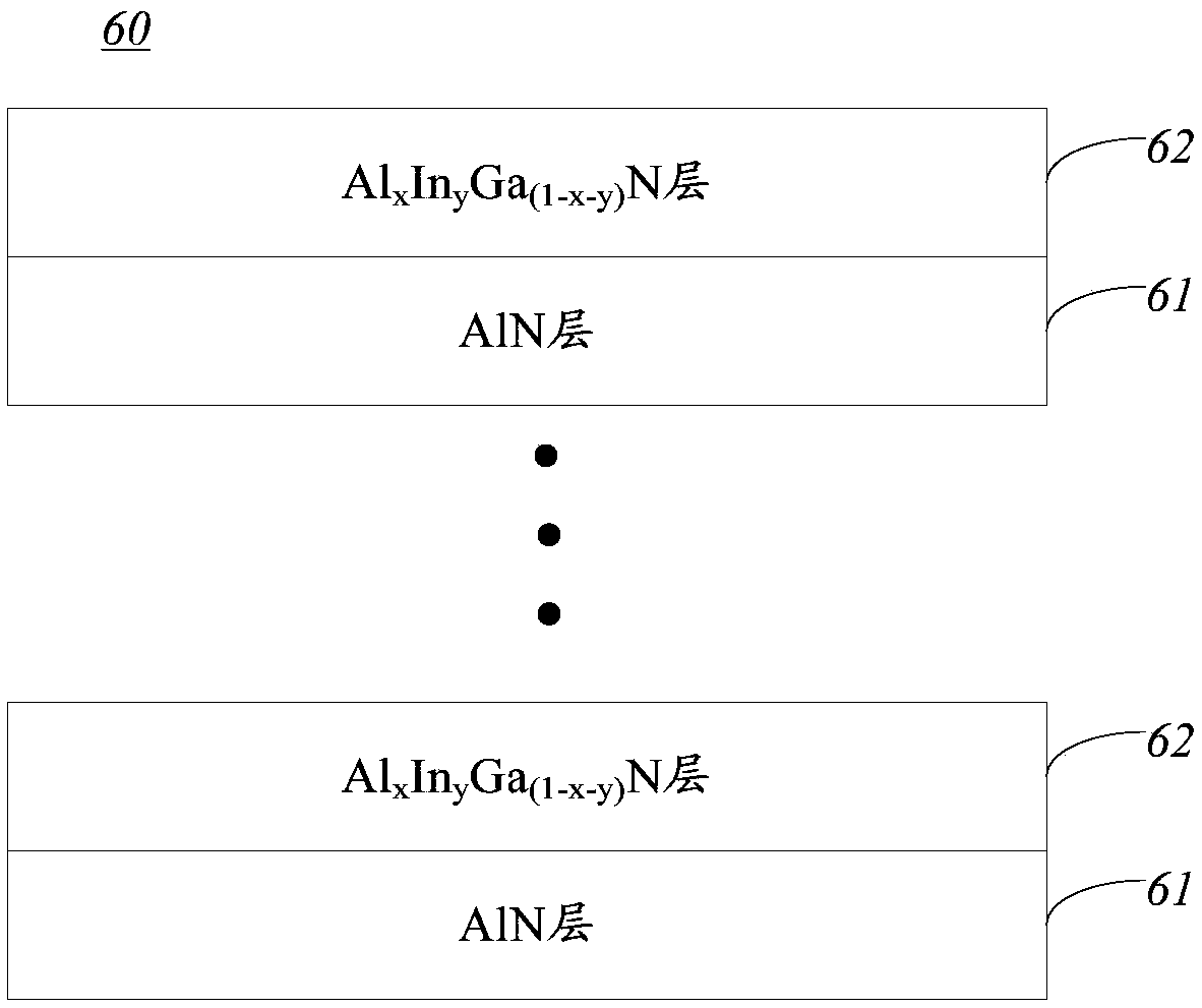
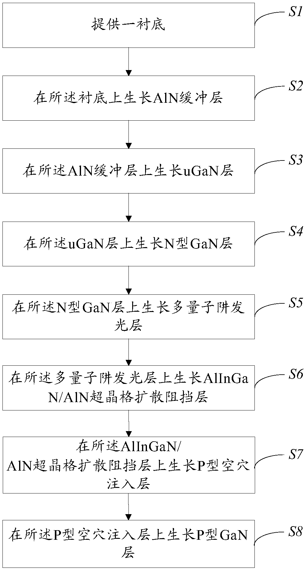
[0039] The LED epitaxial structure 100 includes a substrate 10, an AlN buffer layer 20, a uGaN layer 30, an N-type GaN layer 40, a multiple quantum well light-emitting layer 50, an AlInGaN / AlN superlattice diffusion barrier layer 60, and a P-type hole in order from bottom to top. The injection layer 70 and the P-type GaN layer 80.

[0040] The substrate 10 may be made of sapphire material. Of course, in other embodiments, the substrate 10 may also be made of other substrate ma...


PUM

PropertyMeasurementUnit
Thicknessaaaaaaaaaa
Thicknessaaaaaaaaaa
Thicknessaaaaaaaaaa

Abstract

The invention discloses an LED epitaxial structure and preparation method thereof, the LED epitaxial structure comprises a substrate, an AlN buffer layer, a uGaN layer, an N-type GaN layer, a multi-quantum well light emitting layer, an AlInGaN/AlN superlattice diffusion barrier layer, a P-type hole injection layer and a P-type GaN layer in sequence from bottom to top. As the AlInGaN/AlN superlattice diffusion barrier layer is introduced between the multi-quantum well light emitting layer and the P-type hole injection layer, the P-type doping diffusion can be blocked, the energy level of the conduction band caused by the bending of the energy band can be reduced, the non-radiation recombination of the quantum wells can be reduced, and the effect of the quantum efficiency in the quantum wells can be improved so as to improve the luminous efficiency.

Description

technical field [0001] The invention relates to the technical field of semiconductor light emitting devices, in particular to an LED epitaxial structure and a preparation method thereof. Background technique [0002] Light-emitting diode (Light-Emitting Diode, LED) is a new type of energy-saving and environmentally friendly solid-state lighting source, which has the advantages of high energy efficiency, small size, light weight, fast response speed and long life, so it has been widely used in many fields. Such as solid-state lighting sources, large-screen displays, car tail lights, traffic lights, etc. Among the many applications of LED, it is the most promising one as a general lighting source. One of the core issues of LED lighting is to improve the reliability of LEDs. If a high-reliability LED light source cannot be realized, no matter how good the light effect is, it will limit its application in various fields. Therefore, enhancing LED reliability is the focus of LED...

Claims


Application Information

Patent Timeline
IPC IPC(8): H01L33/00H01L33/14H01L33/32
CPCH01L33/14H01L33/007H01L33/325
Inventor 冯猛刘恒山康双双陈立人
Owner FOCUS LIGHTINGS SCI & TECH
Why Eureka
Try Eureka