Array substrate, driving method, organic light-emitting display panel, and display device

A technology for array substrates and display areas, applied to static indicators, instruments, semiconductor devices, etc., can solve problems such as unfavorable OLED display panels, achieve the effects of simplifying the structure, reducing the occupied area, and improving the afterimage phenomenon

Active Publication Date: 2020-04-17
BOE TECH GRP CO LTD
View PDF5 Cites 0 Cited by
  • Summary
  • Abstract
  • Description
  • Claims
  • Application Information

AI Technical Summary

Problems solved by technology

Due to the limitation of process manufacturing precision, the pixel circuit will occupy a large area in the sub-pixel, which is not conducive to the realization of OLED display panels with high PPI.

Method used


Image

  • Array substrate, driving method, organic light-emitting display panel, and display device
  • Array substrate, driving method, organic light-emitting display panel, and display device
  • Array substrate, driving method, organic light-emitting display panel, and display device

Examples


Embodiment 1

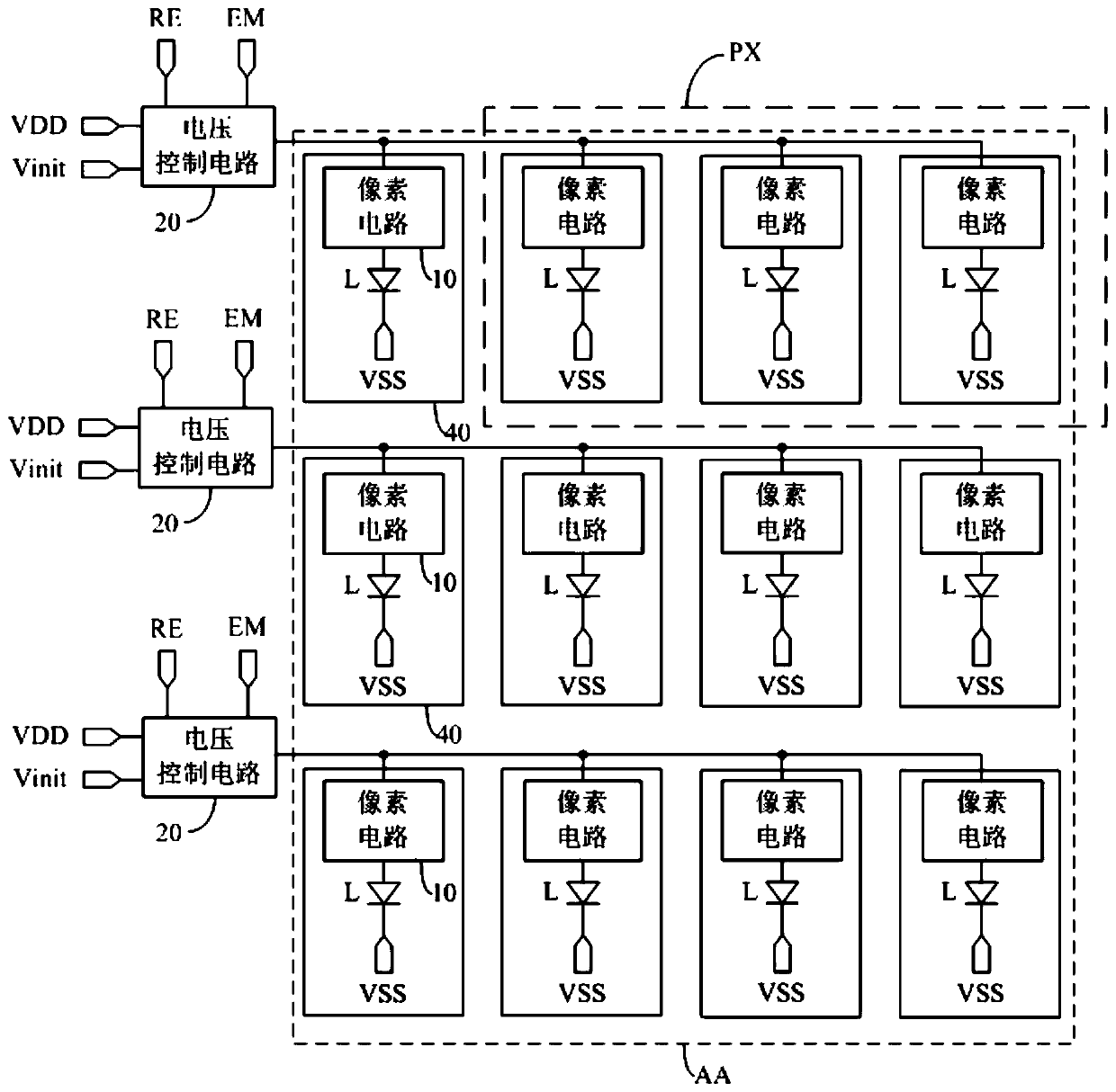
[0080] by Figure 4 The array substrate shown is taken as an example, and the corresponding circuit timing diagram is as follows Figure 7 shown. Driving a row of light emitting devices to work may include: a reset phase T1, a data writing phase T2, and a light emitting phase T3.

[0081] In the reset phase T1, S1=0, S2=1, RE=1, EM=1.

[0082] Since EM=1, the second switching transistor M2 is turned off. Since S1=0, the third switching transistor M3 is turned off. Since S2=1, the fourth switching transistor M4 is turned off. Since RE=1, the first switching transistor M1 is turned on to provide the initialization signal Vinit to the first pole S of the driving transistor M0. It should be noted that, if the previous frame is displayed, the gate G of the driving transistor M0 stores a high-grayscale data signal (that is, displays a high grayscale) through the storage capacitor Cst, then the first electrode S, The voltages of the second pole D and the positive pole of the li...

Embodiment 2

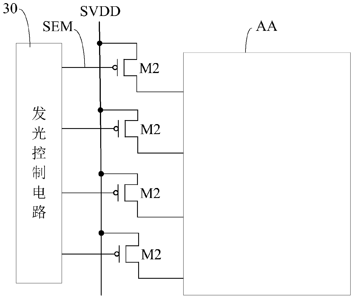
[0088] The schematic diagram of the structure of the array substrate corresponding to this embodiment is as follows: Figure 4 As shown, it is modified for the implementation in the first embodiment. The following only describes the differences between this embodiment and the first embodiment, and the similarities will not be repeated here. In specific implementation, such as Figure 8 As shown, after the light-emitting period T3, driving a row of light-emitting devices to work may also include: a non-light-emitting period T4; wherein, in the non-light-emitting period T4, the voltage control circuit responds to the light-emitting control signal EM, and combines the first power signal with the driving transistor. The first pole is turned off, and the corresponding pixel circuit is controlled to drive the connected light emitting device to stop emitting light.

[0089] Specifically, the corresponding circuit timing diagram is as follows Figure 8 shown. Driving a row of ligh...

Embodiment 3

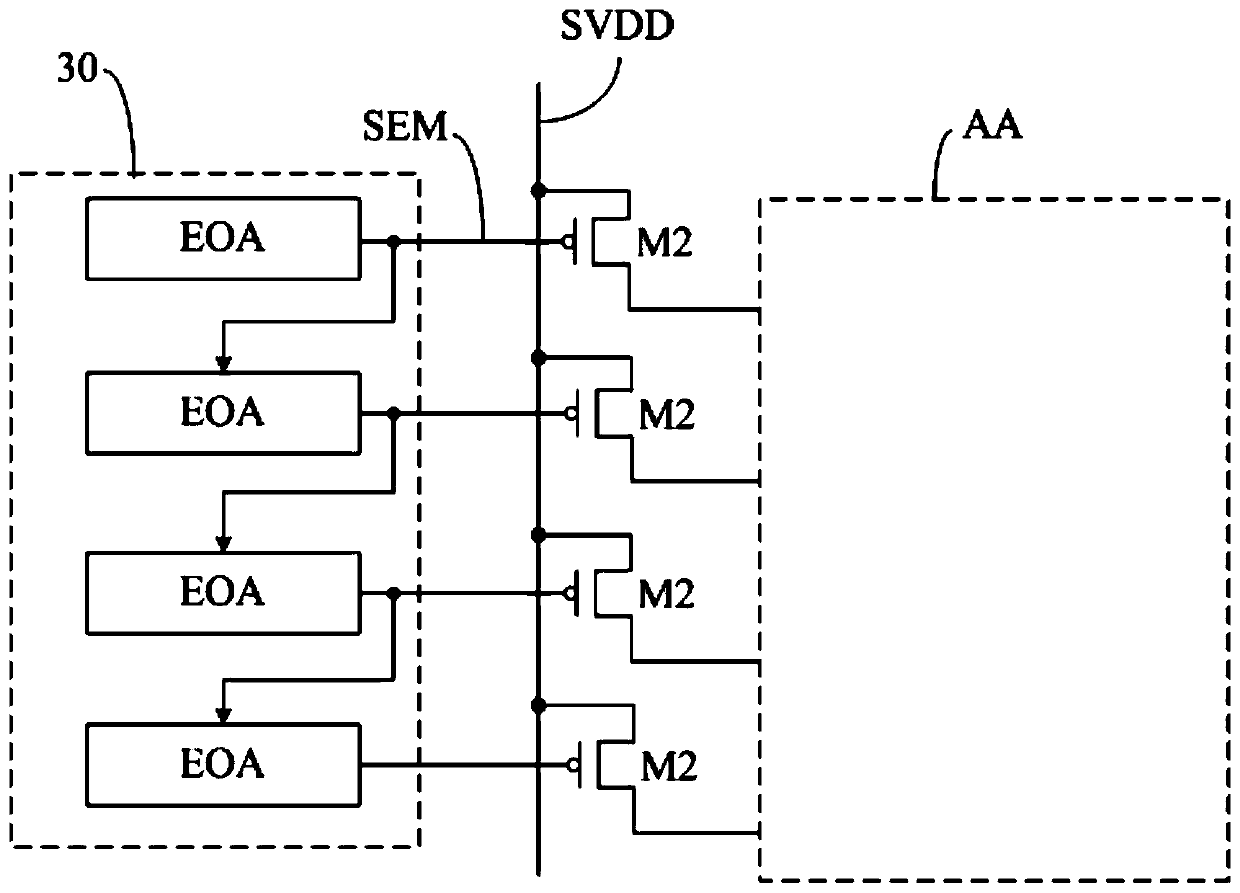
[0092] In specific implementation, such as Figure 9 As shown, within one frame display time Frame, the non-light-emitting phase T4 driving each row of light-emitting devices can be turned on at the same time t0.

[0093] Specifically, a general array substrate may include K rows of pixel units, where K is a positive integer. Gate_k (1 ≤ k ≤ K, and an integer) represents signals for driving the pixel circuit in the pixel unit in the k-th row. Within a frame display time Frame, the pixel circuit can be driven to work by row-by-row driving, and after the light-emitting devices in the first row of pixel units to the last row of pixel units are driven to emit light, then the light-emitting devices in each row of pixel units are controlled simultaneously Stop glowing. For example, when the display time Frame of one frame is 11.1 ms, the non-light-emitting period T4 can be occupied for 2 ms, and the remaining 9.1 ms is the time for driving the pixel circuits in the first row to th...


PUM


Abstract

The invention discloses an array substrate, a driving method, an organic light-emitting display panel and a display device, comprising: a plurality of light-emitting devices located in a display area and a pixel circuit connected to each light-emitting device, and a plurality of voltage electrodes located in a non-display area Control circuit; wherein at least two pixel circuits in one row share one voltage control circuit, so that the structure of each pixel circuit in the display area can be simplified, and the occupied area of ​​the pixel circuits in the display area can be reduced, so that more pixels can be set in the display area A circuit and a light-emitting device to realize a high-PPI organic light-emitting display panel. Moreover, through the control of the reset control signal by the voltage control circuit, the initialization signal is output to the first pole of the driving transistor, and the corresponding light emitting device is controlled to reset, so that the voltage applied to the light emitting device in the previous frame can be avoided from affecting the next frame. The influence of light emission, thereby improving the afterimage phenomenon.

Description

technical field [0001] The present invention relates to the field of display technology, in particular to an array substrate, a driving method, an organic light emitting display panel and a display device. Background technique [0002] Organic light emitting diode (Organic Light Emitting Diode, OLED) display panel is one of the hot spots in the field of flat panel display research today. Compared with liquid crystal display (Liquid Crystal Display, LCD), OLED display has low energy consumption, low production cost, self-illumination, Wide viewing angle and fast response speed etc. advantages. However, the existing OLED display panel includes a plurality of pixel units, and each pixel unit includes a plurality of sub-pixels, and each sub-pixel includes: an OLED and a pixel circuit for driving the OLED to emit light. A pixel circuit generally includes a plurality of transistors and capacitors. Due to the limitation of the manufacturing precision of the process, the pixel cir...

Claims


Application Information

Patent Timeline
Patent Type & Authority Patents(China)
IPC IPC(8): G09G3/3208H01L27/32
CPCG09G3/3208H10K59/353H10K59/12H10K59/131G09G3/3233G09G2300/0842G09G2300/0819G09G2300/0861G09G2310/063G09G2310/0245G09G2300/0465G09G2300/0866G09G3/3266G09G3/3258G09G2310/0286H10K59/1213H10K59/1216
Inventor 杨盛际董学陈小川王辉李胜男郑增强
Owner BOE TECH GRP CO LTD
Why Eureka
Try Eureka