OLED display panel and manufacturing method thereof

A technology for display panels and manufacturing methods, applied in semiconductor/solid-state device manufacturing, electrical components, electric solid-state devices, etc., capable of solving problems such as complex process, high cost, and weak water and oxygen resistance

Inactive Publication Date: 2018-12-18
WUHAN CHINA STAR OPTOELECTRONICS SEMICON DISPLAY TECH CO LTD
View PDF8 Cites 7 Cited by
  • Summary
  • Abstract
  • Description
  • Claims
  • Application Information

AI Technical Summary

Problems solved by technology

[0005] The invention provides an OLED display panel and a manufacturing method thereof to solve the problems of weak water and oxygen resistance, high cost and complicated process on the sides of the existing OLED display panel packaging structure

Method used


Image

  • OLED display panel and manufacturing method thereof
  • OLED display panel and manufacturing method thereof
  • OLED display panel and manufacturing method thereof

Examples


Embodiment Construction

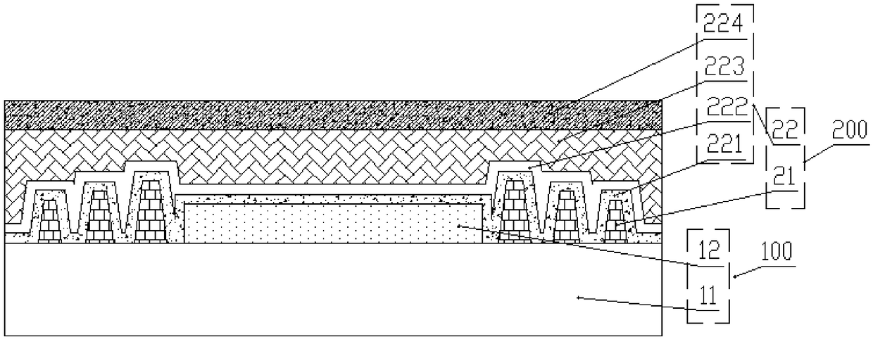
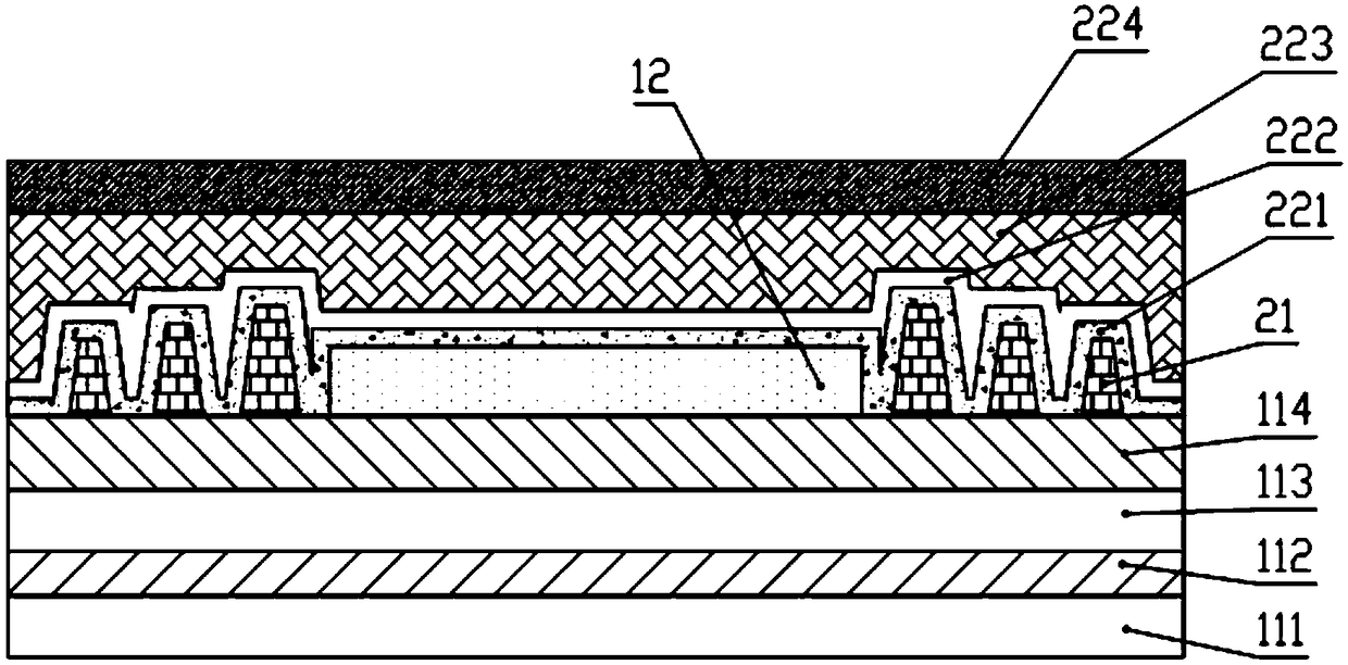
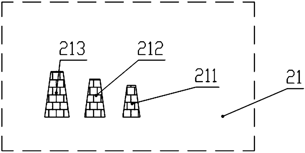
[0038] The following descriptions of the various embodiments refer to the accompanying drawings to illustrate specific embodiments in which the invention may be practiced. The directional terms mentioned in the present invention, such as [top], [bottom], [front], [back], [left], [right], [inside], [outside], [side], etc., are only for reference The orientation of the attached schema. Therefore, the directional terms used are used to illustrate and understand the present invention, but not to limit the present invention. In the figures, structurally similar elements are denoted by the same reference numerals.

[0039] Aiming at the problems of weak water and oxygen resistance, high cost and complicated process on the sides of the existing OLED display panel packaging structure, the present invention proposes a method for manufacturing an OLED display panel and an OLED display panel. This embodiment can improve the defect .

[0040] The present invention will be further descr...


PUM


Abstract

The invention provides an OLED display panel and a manufacturing method thereof, comprising an OLED substrate and a packaging part arranged on the OLED substrate. The OLED substrate comprises a substrate and an OLED layer, wherein the substrate comprises a display area and an edge area surrounding the display area, and the OLED layer is arranged in the display area; The encapsulation part comprises a barrier body and an encapsulation layer. the barrier body is arranged in the edge region and comprises at least one coil of barrier ring. The barrier ring surrounds the OLED layer and spaced fromthe OLED. The encapsulation layer is arranged above the barrier body. By providing a barrier including at least one loop of barrier coils in an edge region of an OLED substrate, The barrier and the inorganic layer are combined to enhance the water-oxygen resistance of the side surface of the OLED display panel, thereby avoiding the multi-layer photomask manufacturing process and simplifying the manufacturing process of the OLED display panel on the basis of improving the water-oxygen resistance of the packaging structure omni-directionally.

Description

technical field [0001] The invention relates to the field of display technology, in particular to an OLED display panel and a manufacturing method thereof. Background technique [0002] Organic light emitting diode (OLED for short) has excellent characteristics such as self-luminescence, low energy consumption, wide viewing angle, rich colors, fast response, etc., and OLEDs can be used to prepare flexible display devices. OLED has therefore aroused great interest in the scientific research community and the industry, and is considered to be a very promising next-generation technology. [0003] Currently, OLED screens widely used in the display field generally adopt a top-emitting (top-emitting) device structure, and an OLED device is composed of an anode, an organic layer and a cathode. Wherein, the organic layer includes a hole injection layer, a hole transport layer, an organic light emitting layer, an electron transport layer and an electron injection layer. [0004] Si...

Claims


Application Information

Patent Timeline
Patent Type & Authority Applications(China)
IPC IPC(8): H01L51/52H01L27/32
CPCH10K59/122H10K50/844H10K71/00
Inventor 郭天福
Owner WUHAN CHINA STAR OPTOELECTRONICS SEMICON DISPLAY TECH CO LTD
Why Eureka
Try Eureka