
Heat dissipating device and method for packaging of high-power semiconductor laser device

A cooling device and semiconductor technology, applied in the direction of semiconductor lasers, lasers, laser components, etc., can solve the problems of low heat dissipation efficiency of the cooling device, achieve excellent heat dissipation effect, compact structure, and realize high-power multi-single-tube laser chip packaging Effect

Active Publication Date: 2019-01-01
CENT SOUTH UNIV
View PDF3 Cites 7 Cited by
  • Summary
  • Abstract
  • Description
  • Claims
  • Application Information

AI Technical Summary

Problems solved by technology

[0008] Aiming at the deficiencies of the prior art, the present invention provides a heat dissipation device and method for high-power semiconductor laser packaging, which solves the problem of low heat dissipation efficiency of existing heat dissipation devices for high-power semiconductor laser packaging

Method used


Image

  • Heat dissipating device and method for packaging of high-power semiconductor laser device
  • Heat dissipating device and method for packaging of high-power semiconductor laser device
  • Heat dissipating device and method for packaging of high-power semiconductor laser device

Examples


Embodiment Construction

[0039] The following will clearly and completely describe the technical solutions in the embodiments of the present invention with reference to the accompanying drawings in the embodiments of the present invention. Obviously, the described embodiments are only some, not all, embodiments of the present invention. Based on the embodiments of the present invention, all other embodiments obtained by persons of ordinary skill in the art without making creative efforts belong to the protection scope of the present invention.

[0040] In describing the present invention, it should be understood that the terms "center", "longitudinal", "transverse", "length", "width", "thickness", "upper", "lower", "front", " Back", "Left", "Right", "Vertical", "Horizontal", "Top", "Bottom", "Inner", "Outer", "Clockwise", "Counterclockwise", "Axial", The orientation or positional relationship indicated by "radial", "circumferential", etc. is based on the orientation or positional relationship shown in...


PUM

PropertyMeasurementUnit
Widthaaaaaaaaaa
Thicknessaaaaaaaaaa

Abstract

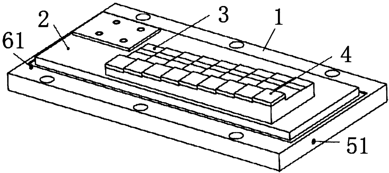
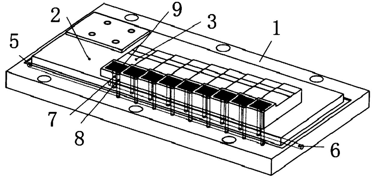
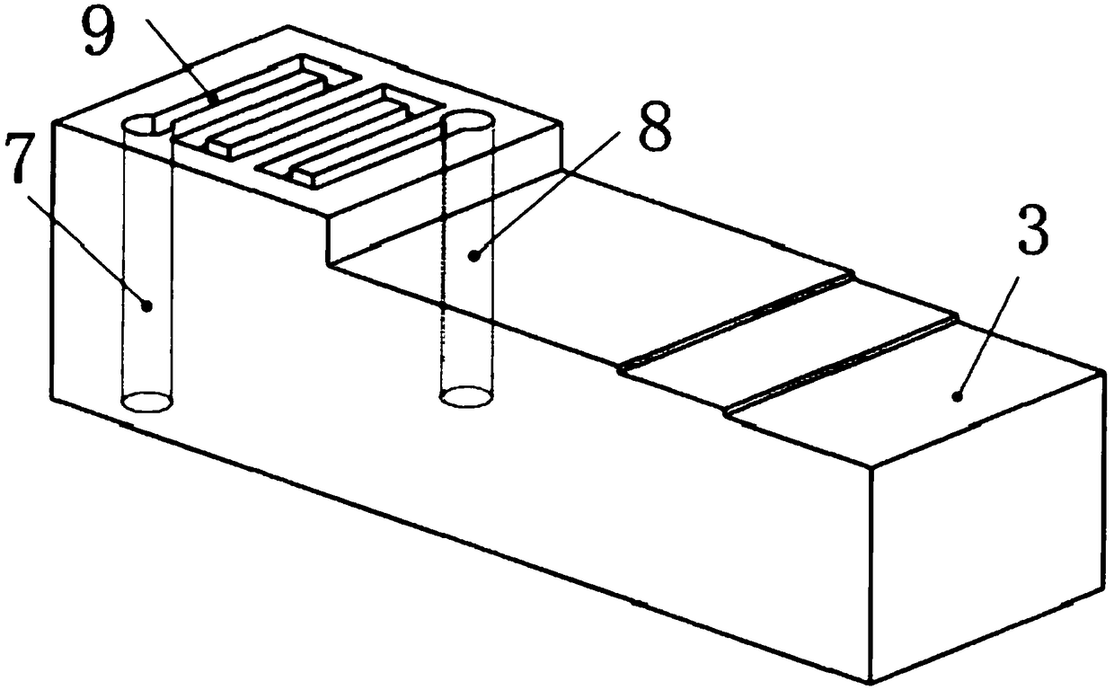
The invention discloses a heat dissipating device for packaging of a high-power semiconductor laser device. The heat dissipating device comprises a bottom plate, a base, and a heat dissipation moduleof a single tube laser chip. A first-level cooling channel liquid inlet pipe and a first-level cooling channel liquid outlet pipe are arranged inside the bottom plate; a final liquid inlet is formed in one side wall of the bottom plate and is communicated with one end of the first-level cooling channel liquid inlet pipe; and a final liquid outlet is formed in the other side wall of the bottom plate and is communicated with the first-level cooling channel liquid outlet pipe. In addition, the invention also discloses a heat dissipating method for packaging of a high-power semiconductor laser device. The heat dissipating method comprises seven steps. According to the invention, a micro-channel heat dissipation structure is formed by three levels of channels; with the third-level micro-channelstructure, the good cooling effect of the high-power multi-single-tube laser device is ensured; and on the basis of the second-level micro channel and the first-level micro channel, a problem of a height difference between the heat dissipating modules is solved, so that processing of the inclination angle is avoided and the uniform heat dissipation is guaranteed.

Description

technical field [0001] The invention relates to the technical field related to semiconductor lasers, in particular to a heat dissipation device and method for packaging high-power semiconductor lasers. Background technique [0002] High-power lasers have a wide range of applications in the fields of industry and national defense. Compared with traditional lamp-pumped lasers, semiconductor lasers have many advantages such as small size, high efficiency, light weight, long life, and low cost, and play an increasingly important role in many aspects of the national economy. The multi-single tube combination of semiconductor lasers is the smallest optical module composed of single laser tubes, which can be directly combined to achieve fiber output. The advantages of multi-single-tube laser beam combining are: long life, high reliability, good slow-axis beam quality, and can be coupled into optical fibers with a core diameter of ≤100 μm; and the overall light source module is sma...

Claims


Application Information

Patent Timeline
IPC IPC(8): H01S5/024
CPCH01S5/02423
Inventor 严一雄郑煜段吉安
Owner CENT SOUTH UNIV
Learn More