Quantum dot electroluminescent device and preparation method thereof

An electroluminescent device and quantum dot light-emitting technology, which is applied in the field of quantum dots, can solve problems such as difficult implementation of the method, and achieve the effects of solving difficult implementation, slowing down transmission, and low manufacturing process requirements

Active Publication Date: 2019-01-04
NANJING TECH CORP LTD
View PDF5 Cites 12 Cited by
  • Summary
  • Abstract
  • Description
  • Claims
  • Application Information

AI Technical Summary

Problems solved by technology

[0007] The main purpose of the present invention is to provide a quantum dot electroluminescent device and its preparation method to solve the problem that the method for balancing the carrier injection of the quantum dot light emitting device in the prior art is difficult to realize

Method used


Image

  • Quantum dot electroluminescent device and preparation method thereof
  • Quantum dot electroluminescent device and preparation method thereof

Examples


preparation example Construction

[0044] According to another aspect of the present application, a method for preparing a quantum dot electroluminescent device is also provided, the method comprising the steps of:

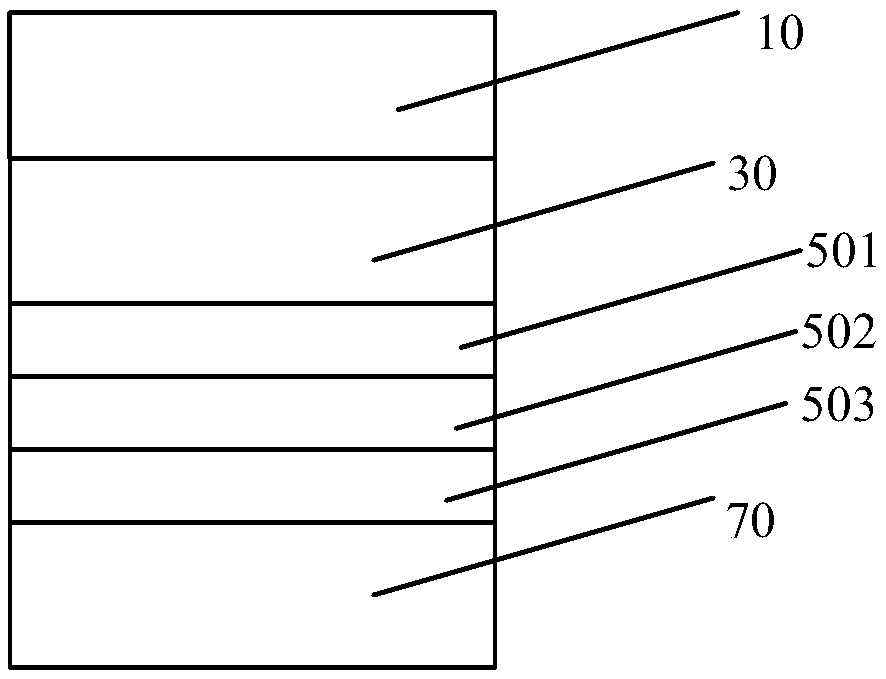
[0045] S1, disposing the first electrode layer 10 on the substrate;

[0046] S2, disposing a quantum dot light-emitting layer 30 on the surface of the first electrode layer 10;

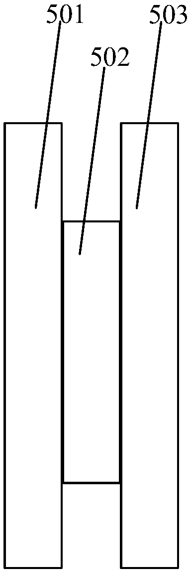
[0047] S3, disposing the functional layer 50 on the surface of the quantum dot light-emitting layer 30 away from the first electrode layer 10, wherein the process of disposing the functional layer 50 includes sequentially laminating and disposing the first A subfunctional layer 501, a second subfunctional layer 502 and a third subfunctional layer 503, wherein the second subfunctional layer 502 includes an electron transport material, and the first subfunctional layer 501 and the third subfunctional layer 503 have corresponding materials The gap widths are respectively greater than the bandgap widths of the electron transp...

Embodiment 1

[0051] The quantum dot electroluminescent device in this embodiment comprises in turn:

[0052] The first electrode layer (ITO cathode, thickness is about 200nm),

[0053] Hole injection layer (PEDOT:PSS, thickness about 40nm),

[0054] A hole transport layer (TFB, about 25nm thick),

[0055] Quantum dot luminescent layer 30 (thickness is about 10nm) formed by red quantum dots,

[0056] The first sub-functional layer 501 (ZrO 2 , the LUMO energy level is about -3.41eV, the HOMO energy level is about -8.41eV, the bandgap width is 4eV, and the thickness is about 20nm), where LUMO is the lowest unoccupied molecular orbital, which is the abbreviation of Lowest Unoccupied Molecular Orbital; HOMO is the highest occupied Molecular Orbital is the abbreviation of Highest Occupied Molecular Orbital.

[0057] The second sub-functional layer 502 (ZnO, the LUMO energy level is about -4.19eV, the HOMO energy level is about -7.39eV, the bandgap width is 3.2eV, and the thickness is about ...

Embodiment 2

[0061] The quantum dot electroluminescent device in this embodiment differs from Embodiment 1 in that:

[0062] Include the first electrode layer (ITO cathode, thickness 200nm) in sequence,

[0063] Hole injection layer (PEDOT:PSS, thickness about 40nm),

[0064] A hole transport layer (TFB, about 25nm thick),

[0065] Quantum dot luminescent layer 30 (thickness 30nm) formed by red quantum dots,

[0066] The first sub-functional layer 501 (NiO, the LUMO energy level is about -4eV, the HOMO energy level is about -7.5eV, the bandgap width is 3.5eV, and the thickness is about 1nm),

[0067] The second sub-functional layer 502 (ZnO, the LUMO energy level is about -4.19eV, the HOMO energy level is about -7.39eV, the bandgap width is 3.2eV, and the thickness is about 20nm),

[0068] The third sub-functional layer (NiO, the LUMO energy level is about -4eV, the HOMO energy level is about -7.5eV, the bandgap width is 3.5eV, and the thickness is about 1nm),

[0069] The second elect...


PUM


Abstract

The invention provides a quantum dot electroluminescent device and a preparation method thereof. The quantum dot electroluminescent device comprises a first electrode layer; a quantum dot light emitting layer disposed on the surface of the first electrode layer; a functional layer disposed on a surface of the quantum dot light emitting layer remote from the first electrode layer, the functional layer includes a first sub-functional layer, a second sub-functional layer and a third sub-functional layer stacked in sequence, the second sub-functional layer comprises an electron transport material,the band gap widths of the materials corresponding to the first and third sub-functional layers are larger than that of the electron transport material, the highest occupied molecular orbital energylevels of the materials corresponding to the first and third sub-functional layers are smaller than that of the electron transport materials, and the lowest unoccupied molecular orbital energy levelsof the materials corresponding to the first and third sub-functional layers are larger than that of the electron transport materials, respectively. A second electrode layer disposed on a surface of the functional layer remote from the quantum dot light emitting layer. By adoption of the quantum dot electroluminescent device, while balanced carrier injection is realized, the material applicabilityis improved.

Description

technical field [0001] The invention relates to the field of quantum dots, in particular to a quantum dot electroluminescent device and a preparation method thereof. Background technique [0002] In the fields of lighting and display, light-emitting diodes (LEDs) have attracted extensive attention due to their advantages of high brightness and low energy consumption. [0003] Currently commercialized semiconductor quantum well structure LEDs include organic semiconductor light-emitting diodes (OLEDs) and quantum dot light-emitting diodes (QD-LEDs), the latter of which is more photochemically stable than organic materials due to the use of quantum dots, and has a narrow half-peak width. , easy to produce by the whole solution method, etc., has become a research hotspot in recent years. [0004] However, the unbalanced carrier injection of QD-LED currently limits its luminous efficiency and lifetime. The current typical quantum dot light-emitting diode structure is a device ...

Claims


Application Information

Patent Timeline
Patent Type & Authority Applications(China)
IPC IPC(8): H01L51/50H01L51/54H01L51/56
CPCH10K85/141H10K85/649H10K85/324H10K50/11H10K2101/40H10K50/115H10K50/166H10K2102/101H10K2102/00H10K2102/102H10K71/00
Inventor 陈涛
Owner NANJING TECH CORP LTD
Why Eureka
Try Eureka