Supercharge Your Innovation With Domain-Expert AI Agents!

a graphite base

A graphite base and pocket technology, applied in the direction of crystal growth, from chemically reactive gases, coatings, etc., can solve the problem of inconsistent light emission wavelengths of epitaxial wafers, etc.

Active Publication Date: 2020-10-27
HC SEMITEK ZHEJIANG CO LTD
View PDF7 Cites 0 Cited by
  • Summary
  • Abstract
  • Description
  • Claims
  • Application Information

AI Technical Summary

Problems solved by technology

[0006] The embodiment of the present invention provides a graphite base, which can solve the problem in the prior art that the substrate is in contact with the side wall of the pocket under the action of centrifugal force, resulting in inconsistent light emission wavelengths in various regions of the epitaxial wafer

Method used


Image

  • a graphite base
  • a graphite base

Examples


Embodiment Construction

[0023] In order to make the object, technical solution and advantages of the present invention clearer, the implementation manner of the present invention will be further described in detail below in conjunction with the accompanying drawings.

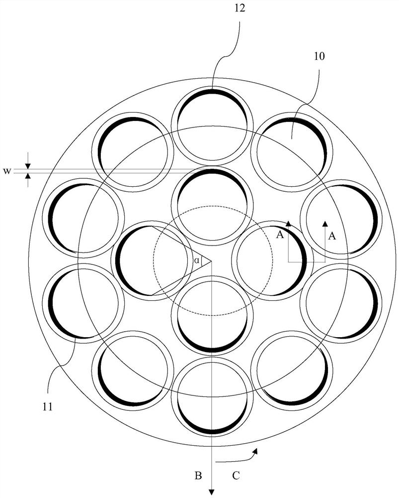
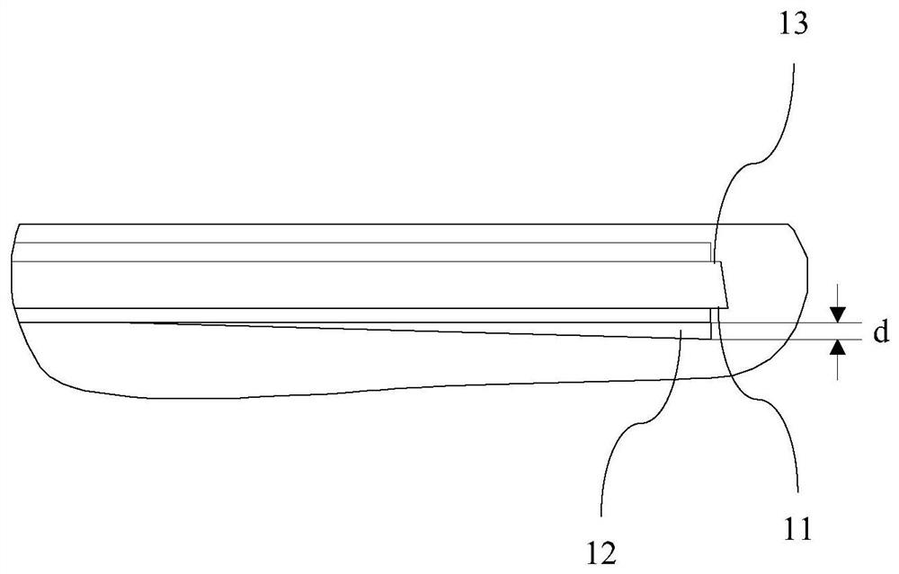
[0024] An embodiment of the present invention provides a graphite base. figure 1 A schematic structural view of a graphite base provided by an embodiment of the present invention, figure 2 for figure 1 A-A cross-sectional view. see figure 1 and figure 2 , the graphite base is provided with a plurality of pockets 10 for accommodating the substrate, and the edge of each pocket 10 is provided with a bump 11 for suspending the substrate in the pocket, and the area surrounded by the bump 11 is in contact with the graphite The farthest part between the centers of the base is provided with grooves 12 .

[0025] In the embodiment of the present invention, a groove is provided at the part farthest from the center of the graphite base in ...


PUM

PropertyMeasurementUnit
depthaaaaaaaaaa
widthaaaaaaaaaa

Abstract

The invention discloses a graphite base, and belongs to the technical field of semiconductors. A plurality of pockets for accommodating substrates are arranged on the graphite base, a bump used for suspending each substrate in each pocket is arranged on the edge of each pocket, and grooves are formed in parts having the furthest distances between the areas surrounded by the bumps and the center ofthe graphite base. According to the invention, the grooves are formed in the parts having the furthest distances between the areas surrounded by the bumps and the center of the graphite base to increase the distance between the parts and the substrates suspended above, thereby reducing the heat conducted to the substrates by the parts to balance elevated temperature because the substrates suspended above the parts are in close contact with the sidewalls of the pockets, so that the temperatures of areas of an epitaxial wafer are balanced, the luminous wavelengths of the areas of the epitaxialwafer are consistent, and the in-chip uniformity and edge yield of the epitaxial wafer are improved.

Description

technical field [0001] The invention relates to the technical field of semiconductors, in particular to a graphite base. Background technique [0002] A semiconductor light-emitting diode (English: Light Emitting Diode, referred to as: LED) is a semiconductor diode that can convert electrical energy into light energy. LED has the advantages of high efficiency, energy saving, and environmental protection, and is widely used in traffic indication, outdoor full-color display and other fields. In particular, the use of high-power LEDs to realize semiconductor solid-state lighting is expected to become a new generation of light sources and enter thousands of households, causing a revolution in the history of human lighting. [0003] The epitaxial wafer is the primary product in the LED manufacturing process. When forming an epitaxial wafer, the substrate is placed on the tray in the reaction chamber of the Metal Organic Chemical Vapor Deposition (English: Metal Organic Chemical...

Claims


Application Information

Patent Timeline
Patent Type & Authority Patents(China)
IPC IPC(8): C23C16/458C30B25/12
CPCC23C16/4581C30B25/12
Inventor 乔楠徐晓波李昱桦刘旺平胡加辉
Owner HC SEMITEK ZHEJIANG CO LTD
Features
  • R&D
  • Intellectual Property
  • Life Sciences
  • Materials
  • Tech Scout
  • Unparalleled Data Quality
  • Higher Quality Content
  • 60% Fewer Hallucinations
Learn More