A manufacture method of an ultraviolet LED light source module

An LED light source and manufacturing method technology, applied in electrical components, circuits, semiconductor devices, etc., can solve the problems of serious light decay, easy gas leakage, poor air tightness, etc., to reduce light decay, improve life, and maintain good air tightness. Effect

Inactive Publication Date: 2019-01-11
深圳优卫乐得科技有限公司
View PDF7 Cites 0 Cited by
  • Summary
  • Abstract
  • Description
  • Claims
  • Application Information

AI Technical Summary

Problems solved by technology

But looking at these pressed modules, there are basically the same problems: 1. The glue is aging, and the metal lens cover falls off; 2. The airtightness is poor, and it is easy to leak; 3. The light decay is serious, and the service life of the lamp beads is short; 4. The power of the chip cannot be increased, and generally can only reach 50% of the designed power of the chip

Method used


Image

  • A manufacture method of an ultraviolet LED light source module
  • A manufacture method of an ultraviolet LED light source module
  • A manufacture method of an ultraviolet LED light source module

Examples


Embodiment Construction

[0028] The technical solutions in the embodiments of the present invention will be clearly and completely described below with reference to the accompanying drawings in the embodiments of the present invention. Obviously, the described embodiments are only a part of the embodiments of the present invention, but not all of the embodiments. Based on the embodiments of the present invention, all other embodiments obtained by those of ordinary skill in the art without creative work fall within the protection scope of the present invention.

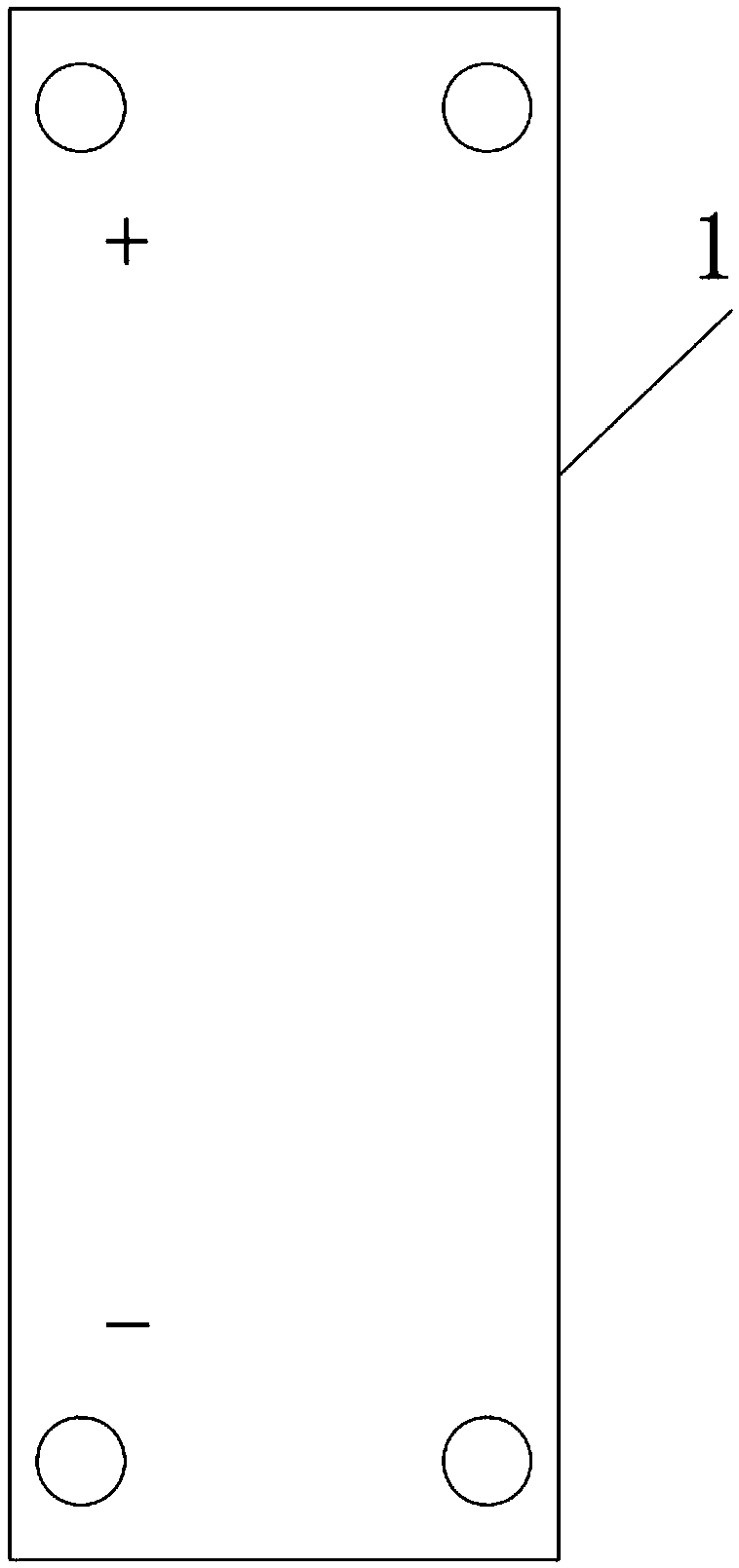
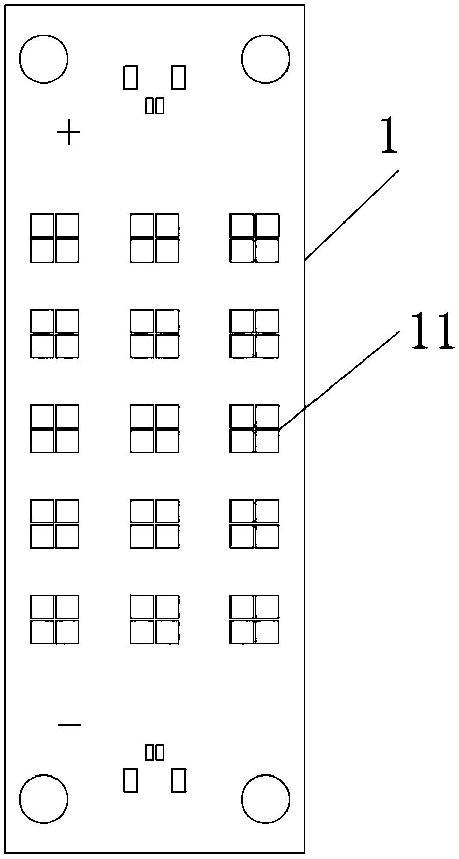
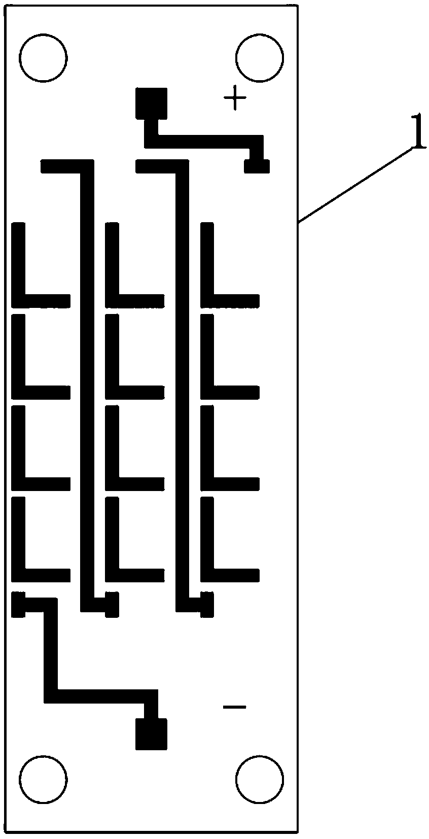
[0029] The present invention provides a method for manufacturing an ultraviolet LED light source module, which comprises the following steps: figure 1 Taking the shown substrate as an example, the specific scheme of the present invention is described in detail below:

[0030] Step 1: Design the PCB diagram on the substrate according to the circuit structure, and then process the wiring slot and the chip bonding position according to the PCB di...


PUM

PropertyMeasurementUnit
Thicknessaaaaaaaaaa

Abstract

A manufacture method of an ultraviolet LED light source module comprises that follow steps of: designing a PCB diagram on a substrate according to a circuit structure, and proces a through-wire grooveand a chip fixing position according to the PCB diagram; 2, coat a conductive adhesive on that die fixing position and the through-wire groove of the chip and on the other side of the substrate; 3, electroplate treatment; 4, sol resistance treatment; 5, coat conductive adhesive on both sides of that substrate; 6, secondary plate treatment, wherein that thickness of the plating layer is determinedby the mounting depth of the lens; 7, carry out die fixing proces automatically by that die fixing machine at the die fixing position of the substrate, and intelligently bonding the die pin and the line in the wire slot by the automatic bonding machine; 8, instal that lens and simultaneously vacuumize the lens. The chip adopts ceramic substrate to dissipate heat, the photoelectric conversion efficiency is increased by 50%, the chip current density is increased by more than 100%, and the light output power is increased by more than 50%.

Description

technical field [0001] The invention relates to the technical field of ultraviolet (UV) LED curing, in particular to a method for manufacturing an ultraviolet LED light source module. Background technique [0002] Ultraviolet (UV)-LED module packaging has a variety of packaging materials and processes, including copper substrate modules, aluminum substrate modules, superconducting aluminum substrate modules, etc.; but they are basically press-fit, that is, chip bonding It is fixed on the base plate, and then the metal lens cover plate is cured with glue, and the cover plate and the base plate are pressed together. However, looking at these laminated modules, there are basically the same problems: 1. The glue is aging, and the metal lens cover falls off; 2. The air tightness is poor, and it is easy to leak; 3. The light decay is serious and the lamp bead has a short service life; 4. The power of the chip cannot go up, generally it can only reach 50% of the design power of th...

Claims


Application Information

Patent Timeline
IPC IPC(8): H01L33/48H01L33/62H01L33/58H01L33/64
CPCH01L33/48H01L33/58H01L33/62H01L33/641H01L2933/0033H01L2933/0058H01L2933/0066H01L2933/0075
Inventor 兰卫国
Owner 深圳优卫乐得科技有限公司
Why Eureka
Try Eureka