

Nonlinear transmittance testing device
A test device and transmittance technology, applied in the field of nonlinear optics, can solve the problems of long time, influence calculation, large spot size, etc., and achieve the effect of shortening measurement time, reducing requirements, and avoiding errors
- Summary
- Abstract
- Description
- Claims
- Application Information
AI Technical Summary
Problems solved by technology
Method used
Image

Examples
Embodiment Construction
[0023] The following will clearly and completely describe the technical solutions in the embodiments of the present invention with reference to the accompanying drawings in the embodiments of the present invention. Obviously, the described embodiments are only some, not all, embodiments of the present invention. Based on the embodiments of the present invention, all other embodiments obtained by persons of ordinary skill in the art without making creative efforts belong to the protection scope of the present invention.
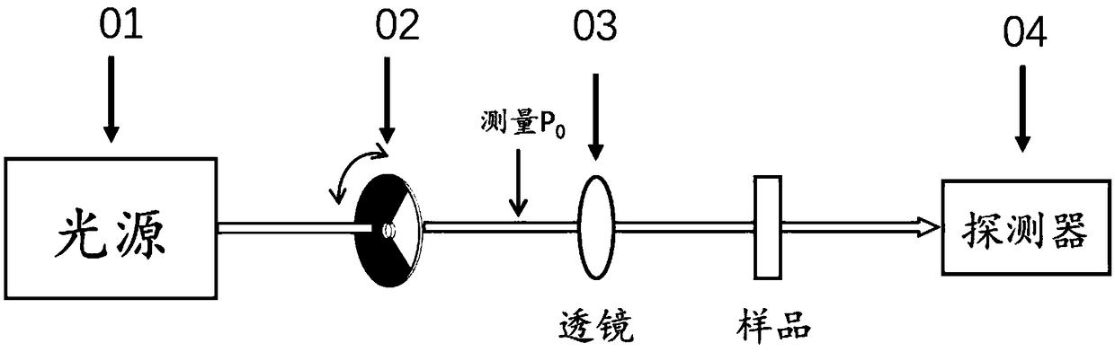
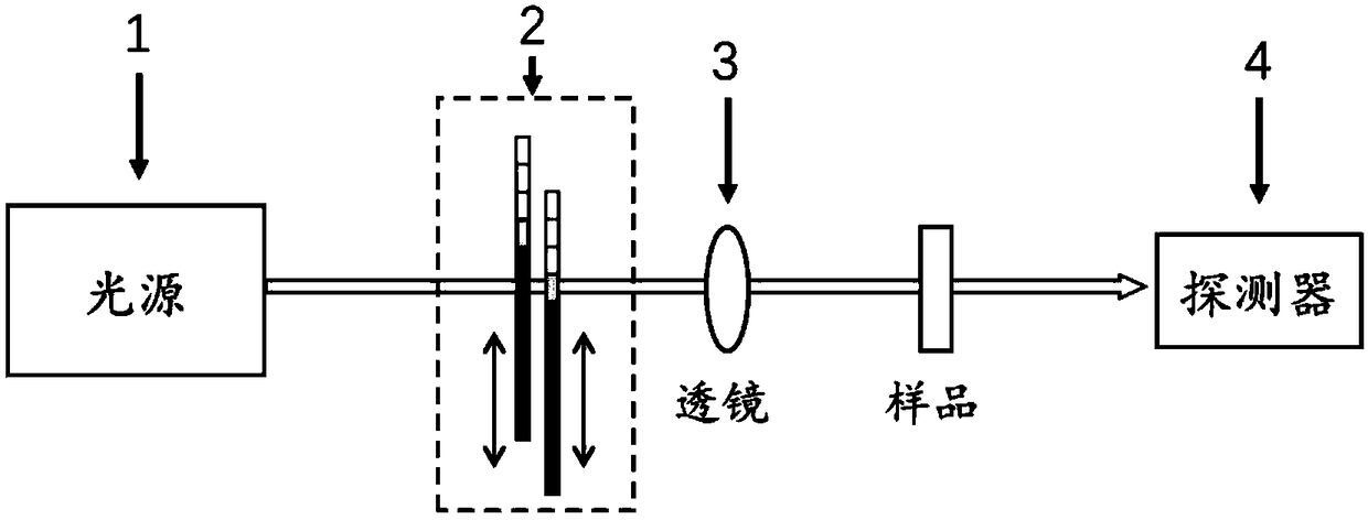
[0024] The invention provides a nonlinear transmittance testing device, such as figure 2 shown, including:
[0025] A light source module 1, configured to provide excitation beams;
[0026] Light intensity attenuation module 2, used to attenuate the excitation beam to a preset power;
[0027] Focusing lens 3, used to focus the attenuated light beam on the sample position;
[0028] The detector 4 is used to measure the nonlinear optical characteristics rela...
PUM
 Abstract
Description
Claims
Application Information