Surface interface passivation layer and passivation method of a kind of crystalline silicon solar cell

A technology of crystalline silicon solar cells and crystalline silicon cells, which is applied in circuits, electrical components, photovoltaic power generation, etc., can solve the problems of low growth rate, achieve reduced interface state density, excellent interface chemical passivation effect, and good field passivation The effect of action

Active Publication Date: 2019-10-11
CHANGZHOU UNIV +1
View PDF17 Cites 0 Cited by
  • Summary
  • Abstract
  • Description
  • Claims
  • Application Information

AI Technical Summary

Problems solved by technology

The disadvantage of ALDS is the extremely slow growth rate

Method used


Image

  • Surface interface passivation layer and passivation method of a kind of crystalline silicon solar cell
  • Surface interface passivation layer and passivation method of a kind of crystalline silicon solar cell
  • Surface interface passivation layer and passivation method of a kind of crystalline silicon solar cell

Examples


example 1

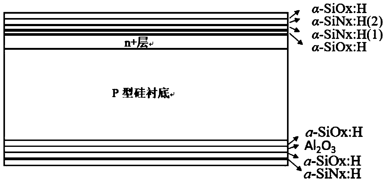
[0030] Example 1: n + α-SiOx:H / α-SiNx:H((refractive index 2.18) / α-SiNx:H(refractive index 2.08) / α-SiOx:H four-layer film passivation on the layer.

[0031] After cleaning the silicon wafer, insert it into the graphite boat, deposit α-SiOx:H layer in the PECVD tube, feed silane and laughing gas, the flow rate of silane is 90sccm, the flow rate of laughing gas is 3.7slm, the temperature is controlled at 450°C, and the pressure is 700mTorr. The power is 2100 watts, and the time is 15s; stop the laughing gas, and turn off the radio frequency source. Keep the temperature controlled at 450°C, increase the flow rate of silane to 500sccm, pass ammonia gas, the flow rate of ammonia gas is 3.8slm, the pressure is 1500mTorr, turn on the radio frequency source, set the radio frequency power to 1700 watts, and deposit the first layer of α-SiNx: H, the time is 550s; then grow the second layer of α-SiOx:H in the PECVD tube, pass ammonia gas, the flow rate of ammonia gas is 4.05slm, the pres...

example 2

[0039] Example 2: α-SiOx:H / Al on p-type layer 2 o 3 / SiOx / α-SiNx:H Quadruple Laminated Thin Film Passivation

[0040] After cleaning the silicon wafer, insert it into the graphite boat, deposit α-SiOx:H layer in the PECVD tube, feed silane and laughing gas, the flow rate of silane is 90sccm, the flow rate of laughing gas is 3.7slm, the temperature is controlled at 450°C, and the pressure is 700mTorr. The power is 2100 watts, and the time is 15s; after the end, the boat is released; it is automatically transferred from the cassette to the ALD chamber to deposit aluminum oxide film, the temperature is controlled at 200°C, and TMA and H 2 O, the flow rates are 10slm and 15slm respectively, and the deposition time is about 15s. After deposition, it is automatically transported out of the chamber and into the cassette. Then the silicon wafer is inserted into the graphite boat, and the second layer of α-SiOx:H layer is grown in the PECVD tube, and silane and laughing gas are intro...

example 3

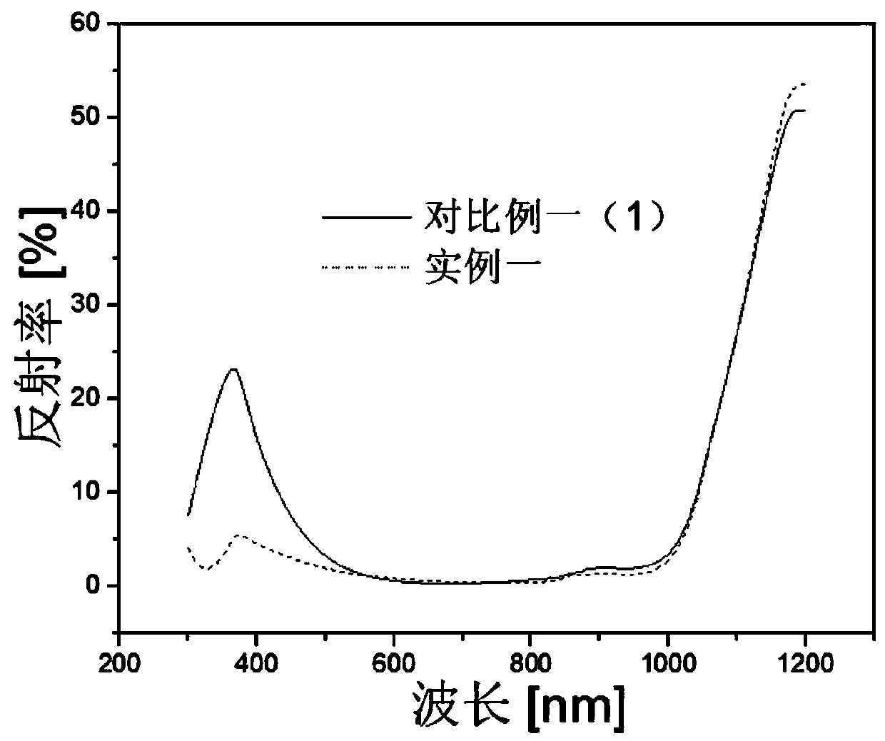
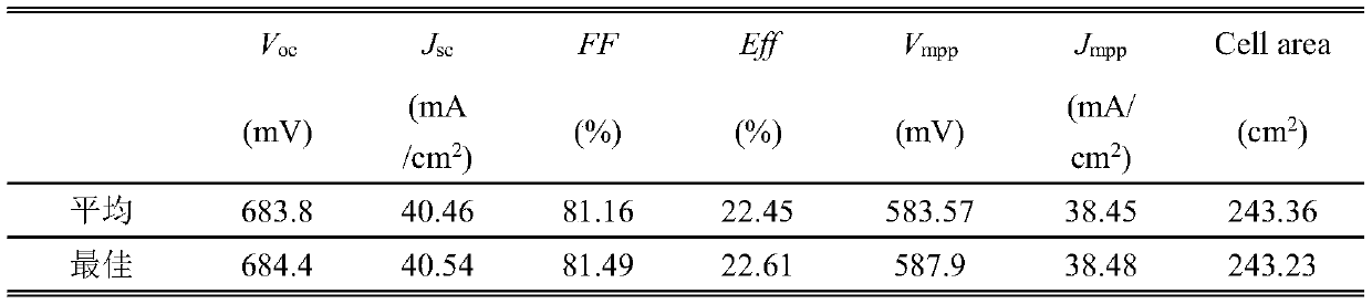
[0051] Example three: the n that embodiment one obtains + Type layer passivation film structure and the application of the p-type layer passivation film structure obtained in Example 2 in p-type PERC cells

[0052] Table 3 Application Effects in Example 3 p-type PERC

[0053]


PUM


Abstract

The invention discloses a surface interface passivation layer of a high-efficiency crystalline silicon solar cell and a passivation method thereof, belonging to the technical field of solar energy manufacturing. An n +-type doping layer is arranged on the front surface of the p-type crystal silicon battery, and the surface of the n +-type doping layer and the surface of the p-type layer on the back surface of the p-type silicon substrate are passivated respectively. Plasma enhanced chemical vapor deposition (PECVD) technique was used to prepare four-layer passivation film on the n + layer of P-type silicon substrate. Plasma enhanced chemical vapor deposition (PECVD) and atomic layer deposition (ALD) were used to prepare a four-layer passivation film on the p-type layer on the back surfaceof P-type silicon substrate, The structure order of the laminated passivation layer prepared by the patent of the invention has a vital effect on the passivation effect, and the laminated layers havemutual synergistic effect, and after passivation, the laminated passivation layer has excellent anti-reflection effect and good passivation effect, and the laminated passivation layer has excellent application prospect in p-type PERC batteries.

Description

technical field [0001] The invention belongs to the technical field of solar energy manufacturing, and relates to a surface interface passivation layer of a high-efficiency crystalline silicon solar cell and a passivation method thereof. It specifically relates to a p-type crystalline silicon cell through the front surface phosphorus diffusion to form n + / p structure, the surface interface passivation method of its front and back. Background technique [0002] Due to surface and interface defects and surface dangling bonds of crystalline silicon solar cells, photogenerated carriers recombine severely at the surface and interface, which leads to a decrease in solar cell efficiency. Effective minority carrier lifetime τ of solar cells eff The lifetime τ of silicon wafer bulk , the effective life of the upper surface τ tsurface and back surface effective lifetime τ bsurface jointly determined, the relationship is: 1 / τ eff =1 / τ bulk +1 / τ tsurface +1 / τ bsurface . With ...

Claims


Application Information

Patent Timeline
Patent Type & Authority Patents(China)
IPC IPC(8): H01L31/0216H01L31/18
CPCH01L31/02167H01L31/1804H01L31/1868Y02E10/547Y02P70/50
Inventor 丁建宁袁宁一叶枫
Owner CHANGZHOU UNIV
Why Eureka
Try Eureka