Micronano-scale high-temperature laser impact imprinting device and method

A laser shock and micro-nano-scale technology, which is applied in laser welding equipment, welding equipment, metal processing equipment, etc., can solve the problems of performance degradation of micro-nano devices, small depth and width of micro-nano structures, and poor replication accuracy, so as to avoid The effect of surface oxidation, large imprint depth, and high manufacturing precision

Pending Publication Date: 2019-01-18
XUZHOU UNIV OF TECH
View PDF0 Cites 13 Cited by
  • Summary
  • Abstract
  • Description
  • Claims
  • Application Information

AI Technical Summary

Problems solved by technology

However, in the process of laser shock imprinting, there are still two problems: first, when laser shock imprinting is performed at room temperature or at a higher temperature (below the recrystallization temperature of the metal material), the obtained metal material The depth-width ratio of the micro-nano structure is small, and the replication accuracy is poor. When the laser focus energy is further increased, t

Method used


Image

  • Micronano-scale high-temperature laser impact imprinting device and method

Examples


Embodiment Construction

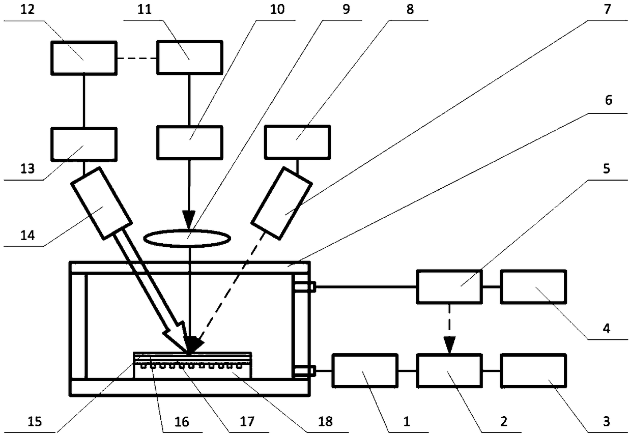
[0027] like figure 1 As shown, a micro-nano-scale high-temperature laser shock imprinting device includes an atmosphere protection module, a high-temperature laser shock imprinting module, a monitoring module and a fixture module. Wherein, the atmosphere protection module includes a target chamber 6. The target chamber 6 has an air inlet and an exhaust port. The oxygen sensor 5 is connected with the exhaust valve 4; and the oxygen sensor 5 is connected with the air pump 2. The high-temperature laser shock embossing module is composed of a focusing mirror 9, a pulse laser 10, a pulse laser controller 11, a pulse delay generator 12, an infrared laser controller 13, and an infrared laser 14; the monitoring module is connected by a CCD 7 and a computer 8 in sequence; The fixture modules are constrained layer 15 , absorbing layer 16 , sample 17 and mold 18 from top to bottom; the fixture module is set in the target chamber; the high-temperature laser shock embossing module is set ...


PUM

PropertyMeasurementUnit
Thicknessaaaaaaaaaa
Thicknessaaaaaaaaaa
Widthaaaaaaaaaa

Abstract

The invention discloses a micronano-scale high-temperature laser impact imprinting device and method, and relates to the technical field of laser impact imprinting. The device comprises an atmosphereprotection module, a high-temperature laser impact imprinting module, a monitoring module and a clamp module; the atmosphere protection module comprises a target chamber, the target chamber is provided with an air inlet and an air outlet, and the air inlet is sequentially connected with an air inlet valve, an air pump and an air storage system through pipelines; the air outlet is connected with anoxygen sensor and an exhaust valve through pipelines; the oxygen sensor is connected with the air pump; the high-temperature laser impact imprinting module is formed by connecting a focus lens, a pulse laser device, a pulse laser controller, a pulse delay generator, an infrared laser controller and an infrared laser device in sequence; the monitoring module is formed by sequentially connecting aCCD and a computer; the clamp module is composed of a constraint layer, an absorption layer, a sample and a mold from top to bottom in sequence; the clamp module is arranged in the target chamber. Laser impact imprinting and rapid manufacturing of a high-precision micronano complex structure on the surface of a metal material are achieved.

Description

technical field [0001] The invention relates to the technical field of laser shock imprinting, in particular to a micro-nano scale high-temperature laser shock imprinting device and method. Background technique [0002] With the rapid development of micro-electromechanical systems, nano-electromechanical systems, and microfluidic chips, higher and higher requirements are placed on the miniaturization and high precision of devices. In the manufacture of micro-devices based on metal materials, how to obtain complex structures at the micro-nano scale on the surface of the material is a relatively big challenge. Laser shock imprinting technology uses high-energy shock waves generated by laser ablation of the absorbing layer to act on the surface of metal materials. Under the action of shock waves, metal materials produce superplastic deformation, which can quickly replicate micro-nano complex structures. However, in the process of laser shock imprinting, there are still two pro...

Claims


Application Information

Patent Timeline
IPC IPC(8): B23K26/356B23K26/18B23K26/12
CPCB23K26/356B23K26/123B23K26/127B23K26/18
Inventor 赵恩兰郭华锋张磊张宁王磊
Owner XUZHOU UNIV OF TECH
Why Eureka
Try Eureka