

A liquid crystal light switch for optical phased array scanning
An optical phased array and optical switch technology, applied in the field of optical phased array, can solve the problems of not being able to use beam phase modulation, not being able to electronically control scanning and deep focus control, etc.
- Summary
- Abstract
- Description
- Claims
- Application Information
AI Technical Summary
Problems solved by technology
Method used
Image

Examples
Embodiment Construction
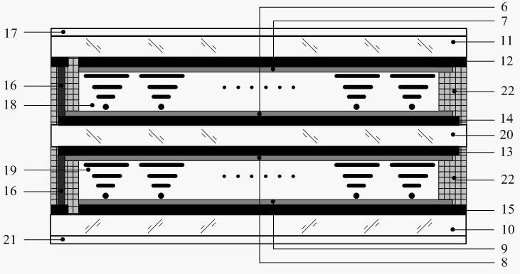
[0031] Such as figure 1 , 2 , 3 and 4, the present invention is composed of a first layer of liquid crystal panel 18 and a second layer of liquid crystal panel 19 arranged up and down, and the first layer of liquid crystal panel 18 is successively provided with row first orientation film 7, Row scanning electrode 12, upper layer glass plate 11 and upper polarizing plate 17, the second alignment film 6, row signal electrode 14 and middle glass plate 20 are arranged in parallel successively below the first layer liquid crystal plate 18; The second layer liquid crystal plate 19 The third alignment film 8 and the column scanning electrode 13 are arranged in parallel on the top, and the fourth alignment film 9, the column signal electrode 15, the lower glass plate 10 and the lower polarizer 21 are arranged in parallel on the bottom of the second layer of liquid crystal panel 19; The row signal electrodes 14 and the column signal electrodes 15 are respectively connected with electr...
PUM
 Abstract
Description
Claims
Application Information